SLAS411D November 2004 – February 2016 DAC8811
PRODUCTION DATA.
- 1 Features
- 2 Applications
- 3 Description
- 4 Revision History
- 5 Device Comparison Table
- 6 Pin Configuration and Functions
- 7 Specifications
- 8 Detailed Description
- 9 Application and Implementation
- 10Power Supply Recommendations
- 11Layout
- 12Device and Documentation Support
- 13Mechanical, Packaging, and Orderable Information
封装选项
机械数据 (封装 | 引脚)
散热焊盘机械数据 (封装 | 引脚)
- DRB|8
订购信息
7 Specifications
7.1 Absolute Maximum Ratings
over operating free-air temperature range (unless otherwise noted)(1)(1) Stresses above those listed under absolute maximum ratings may cause permanent damage to the device. Exposure to absolute maximum conditions for extended periods may affect device reliability.
7.2 ESD Ratings
| MAX | UNIT | |||
|---|---|---|---|---|
| V(ESD) | Electrostatic discharge | Human body model (HBM), per ANSI/ESDA/JEDEC JS-001(1) | ±4000 | V |
| Charged device model (CDM), per JEDEC specification JESD22-C101(2) | ±1000 | |||
(1) JEDEC document JEP155 states that 500-V HBM allows safe manufacturing with a standard ESD control process.
(2) JEDEC document JEP157 states that 250-V CDM allows safe manufacturing with a standard ESD control process.
7.3 Recommended Operating Conditions
over operating free-air temperature range (unless otherwise noted)| MIN | NOM | MAX | UNIT | ||
|---|---|---|---|---|---|
| Supply voltage to GND | 2.7 | 5.5 | V | ||
| Operating ambient temperature, TA | –40 | 125 | °C | ||
7.4 Thermal Information
| THERMAL METRIC(1) | DAC8811 | UNIT | ||
|---|---|---|---|---|
| DGK (VSSOP) | DRB (VSON) | |||
| 8 PINS | 8 PINS | |||
| RθJA | Junction-to-ambient thermal resistance | 169.6 | 46.7 | °C/W |
| RθJC(top) | Junction-to-case (top) thermal resistance | 64.2 | 61.3 | °C/W |
| RθJB | Junction-to-board thermal resistance | 90.3 | 22 | °C/W |
| ψJT | Junction-to-top characterization parameter | 7.7 | 1.1 | °C/W |
| ψJB | Junction-to-board characterization parameter | 88.8 | 22.1 | °C/W |
| RθJC(bot) | Junction-to-case (bottom) thermal resistance | N/A | 3.8 | °C/W |
(1) For more information about traditional and new thermal metrics, see the Semiconductor and IC Package Thermal Metrics application report, SPRA953.
7.5 Electrical Characteristics
VDD = 2.7 V to 5.5 V; IOUT = Virtual GND, GND = 0 V; VREF = 10 V; TA = full operating temperature. All specifications -40°C to 85°C, unless otherwise noted.| PARAMETER | TEST CONDITIONS | MIN | TYP | MAX | UNIT | |
|---|---|---|---|---|---|---|
| STATIC PERFORMANCE | ||||||
| Resolution | 16 | Bits | ||||
| Relative accuracy | DAC8811C | ±1 | LSB | |||
| Relative accuracy | DAC8811B | ±2 | LSB | |||
| Differential nonlinearity | ±0.5 | ±1 | LSB | |||
| Output leakage current | Data = 0000h, TA = 25°C | 10 | nA | |||
| Output leakage current | Data = 0000h, TA = TMAX | 10 | nA | |||
| Full-scale gain error | All ones loaded to DAC register | ±1 | ±4 | mV | ||
| Full-scale tempco | ±3 | ppm/°C | ||||
| OUTPUT CHARACTERISTICS(1) | ||||||
| Output current | 2 | mA | ||||
| Output capacitance | Code dependent | 50 | pF | |||
| REFERENCE INPUT(1) | ||||||
| VREF Range | –15 | 15 | V | |||
| Input resistance | 5 | kΩ | ||||
| Input capacitance | 5 | pF | ||||
| LOGIC INPUTS AND OUTPUT(1) | ||||||
| VIL | Input low voltage | VDD = 2.7V | 0.6 | V | ||
| VDD = 5V | 0.8 | V | ||||
| VIH | Input high voltage | VDD = 2.7V | 2.1 | V | ||
| VDD = 5V | 2.4 | V | ||||
| IIL | Input leakage current | 10 | µA | |||
| CIL | Input capacitance | 10 | pF | |||
| POWER REQUIREMENTS | ||||||
| VDD | 2.7 | 5.5 | V | |||
| IDD (normal operation) | Logic inputs = 0 V | 5 | µA | |||
| VDD = 4.5 V to 5.5 V | VIH = VDD and VIL = GND | 3 | 5 | µA | ||
| VDD = 2.7 V to 3.6 V | VIH = VDD and VIL = GND | 1 | 2.5 | µA | ||
| AC CHARACTERISTICS(1) (2) | ||||||
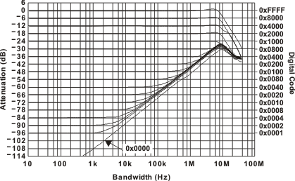
| BW –3 dB | Reference mutiplying BW | VREF = 5 VPP, Data = FFFFh | 10 | MHz | ||
| DAC glitch impulse | VREF = 0 V to 10 V, Data = 7FFFh to 8000h to 7FFFh | 2 | nV/s | |||
| Feed through error VOUT/VREF | Data = 0000h, VREF = 100 mVRMS, f = 100kHz | –70 | dB | |||
| Digital feed through | CS = 1 and fCLK = 1 MHz | 2 | nV/s | |||
| Total harmonic distortion | VREF = 5 VPP, Data = FFFFh, f = 1 kHz | –105 | dB | |||
| Output spot noise voltage | f = 1 kHz, BW = 1 Hz | 12 | nV/√Hz | |||
(1) Specified by design and characterization; not production tested.
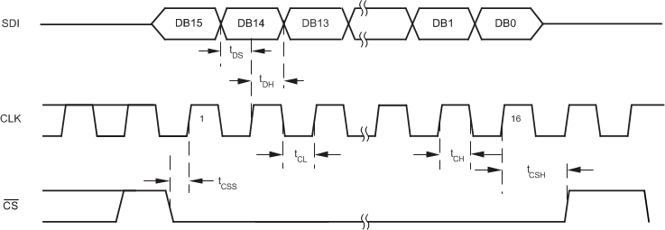
7.6 Timing Requirements
| MIN | NOM | MAX | UNIT | |||
|---|---|---|---|---|---|---|
| INTERFACE TIMING | ||||||
| fCLK | Clock input frequency | 50 | MHz | |||
| t(CH) | Clock pulse width high | 10 | ns | |||
| t(CL) | Clock pulse width low | 10 | ns | |||
| t(CSS) | CS to Clock setup time | 0 | ns | |||
| t(CSH) | Clock to CS hold time | 10 | ns | |||
| t(DS) | Data setup time | 5 | ns | |||
| t(DH) | Data hold time | 10 | ns | |||
| AC CHARACTERISTICS(1) (2) | ||||||
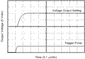
| ts | Output voltage settling time | To ±0.1% of full-scale, Data = 0000h to FFFFh to 0000h | 0.3 | µs | ||
| To ±0.0015% of full-scale, Data = 0000h to FFFFh to 0000h | 0.5 | µs | ||||
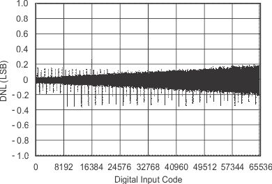
7.7 Typical Characteristics: VDD = 5 V
At TA = 25°C, +VDD = 5 V, unless otherwise noted.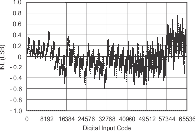
| TA = 25°C |
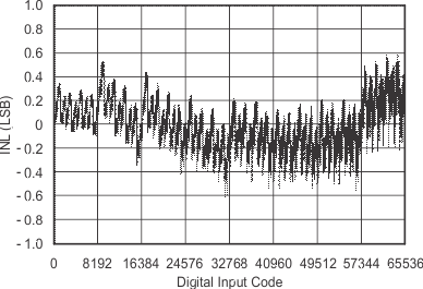
| TA = –40°C |
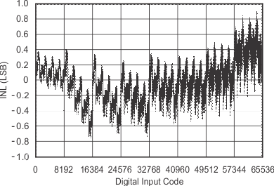
| TA = 85°C |
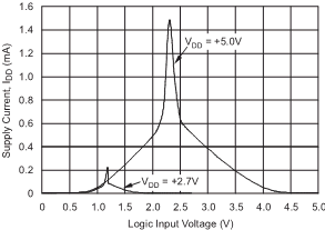
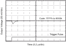
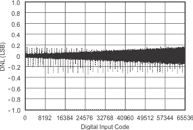
7.8 Typical Characteristics: VDD = 2.7 V
At TA = 25°C, +VDD = 2.7 V, unless otherwise noted.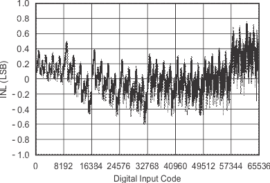
| TA = 25°C |
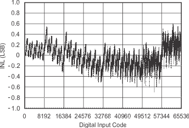
| TA = –40°C |
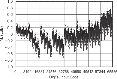
| TA = 85°C |

| TA = 25°C |
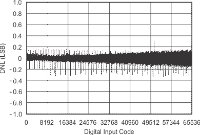
| TA = –40°C |
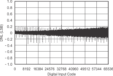
| TA = 85°C |
