ZHCSHA4B July 2007 – January 2018 DAC8881
PRODUCTION DATA.
- 1 特性
- 2 应用
- 3 说明
- 4 修订历史记录
- 5 Pin Configuration and Functions
- 6 Specifications
-
7 Detailed Description
- 7.1 Overview
- 7.2 Functional Block Diagram
- 7.3 Feature Description
- 7.4 Device Functional Modes
- 8 Application and Implementation
- 9 Power Supply Recommendations
- 10Layout
- 11器件和文档支持
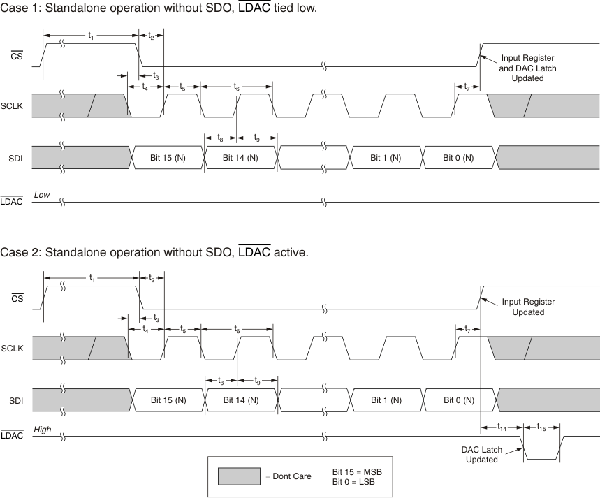
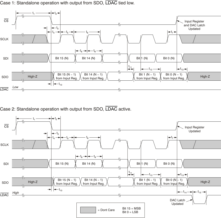
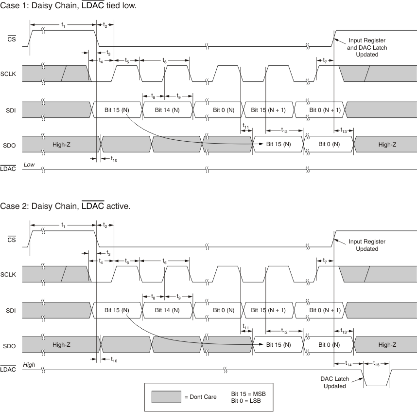
6.7 Timing Characteristics for Figure 2 and Figure 3(1)(2)(3)
At –40°C to +105°C, unless otherwise noted.| PARAMETER | CONDITIONS | MIN | MAX | UNIT | |
|---|---|---|---|---|---|
| fSCLK | Maximum clock frequency | 2.7 ≤ DVDD< 3.6 V, 2.7 ≤ IOVDD ≤ DVDD | 20 | MHz | |
| 3.6 ≤ DVDD ≤ 5.5 V, 2.7 ≤ IOVDD ≤ DVDD | 25 | MHz | |||
| t1 | Minumum CS high time | 2.7 ≤ DVDD< 3.6 V, 2.7 ≤ IOVDD ≤ DVDD | 50 | ns | |
| 3.6 ≤ DVDD ≤ 5.5 V, 2.7 ≤ IOVDD ≤ DVDD | 30 | ns | |||
| t2 | CS falling edge to SCLK rising edge | 2.7 ≤ DVDD< 3.6 V, 2.7 ≤ IOVDD ≤ DVDD | 10 | ns | |
| 3.6 ≤ DVDD ≤ 5.5 V, 2.7 ≤ IOVDD ≤ DVDD | 8 | ns | |||
| t3 | SCLK falling edge to CS falling edge setup time | 2.7 ≤ DVDD< 3.6 V, 2.7 ≤ IOVDD ≤ DVDD | 10 | ns | |
| 3.6 ≤ DVDD ≤ 5.5 V, 2.7 ≤ IOVDD ≤ DVDD | 10 | ns | |||
| t4 | SCLK low time | 2.7 ≤ DVDD< 3.6 V, 2.7 ≤ IOVDD ≤ DVDD | 25 | ns | |
| 3.6 ≤ DVDD ≤ 5.5 V, 2.7 ≤ IOVDD ≤ DVDD | 20 | ns | |||
| t5 | SCLK high time | 2.7 ≤ DVDD< 3.6 V, 2.7 ≤ IOVDD ≤ DVDD | 25 | ns | |
| 3.6 ≤ DVDD ≤ 5.5 V, 2.7 ≤ IOVDD ≤ DVDD | 20 | ns | |||
| t6 | SCLK cycle time | 2.7 ≤ DVDD< 3.6 V, 2.7 ≤ IOVDD ≤ DVDD | 50 | ns | |
| 3.6 ≤ DVDD ≤ 5.5 V, 2.7 ≤ IOVDD ≤ DVDD | 40 | ns | |||
| t7 | SCLK rising edge to CS rising edge | 2.7 ≤ DVDD< 3.6 V, 2.7 ≤ IOVDD ≤ DVDD | 10 | ns | |
| 3.6 ≤ DVDD ≤ 5.5 V, 2.7 ≤ IOVDD ≤ DVDD | 10 | ns | |||
| t8 | Input data setup time | 2.7 ≤ DVDD< 3.6 V, 2.7 ≤ IOVDD ≤ DVDD | 5 | ns | |
| 3.6 ≤ DVDD ≤ 5.5 V, 2.7 ≤ IOVDD ≤ DVDD | 5 | ns | |||
| t9 | Input data hold time | 2.7 ≤ DVDD< 3.6 V, 2.7 ≤ IOVDD ≤ DVDD | 5 | ns | |
| 3.6 ≤ DVDD ≤ 5.5 , 2.7 ≤ IOVDD ≤ DVDD | 5 | ns | |||
| t10 | SDO active from CS falling edge | 2.7 ≤ DVDD< 3.6 V, 2.7 ≤ IOVDD ≤ DVDD | 15 | ns | |
| 3.6 ≤ DVDD ≤ 5.5 V, 2.7 ≤ IOVDD ≤ DVDD | 10 | ns | |||
| t11 | SDO data valid from SCLK falling edge | 2.7 ≤ DVDD< 3.6 V, 2.7 ≤ IOVDD ≤ DVDD | 20 | ns | |
| 3.6 ≤ DVDD ≤ 5.5 V, 2.7 ≤ IOVDD ≤ DVDD | 15 | ns | |||
| t12 | SDO data hold from SCLK rising edge | 2.7 ≤ DVDD< 3.6 V, 2.7 ≤ IOVDD ≤ DVDD | 25 | ns | |
| 3.6 ≤ DVDD ≤ 5.5 V, 2.7 ≤ IOVDD ≤ DVDD | 20 | ns | |||
| t13 | SDO High-Z from CS rising edge | 2.7 ≤ DVDD< 3.6 V, 2.7 ≤ IOVDD ≤ DVDD | 8 | ns | |
| 3.6 ≤ DVDD ≤ 5.5 V, 2.7 ≤ IOVDD ≤ DVDD | 5 | ns | |||
| t14 | CS rising edge to LDAC falling edge | 2.7 ≤ DVDD< 3.6 V, 2.7 ≤ IOVDD ≤ DVDD | 10 | ns | |
| 3.6 ≤ DVDD ≤ 5.5 V, 2.7 ≤ IOVDD ≤ DVDD | 5 | ns | |||
| t15 | LDAC pulse width | 2.7 ≤ DVDD< 3.6 V, 2.7 ≤ IOVDD ≤ DVDD | 15 | ns | |
| 3.6 ≤ DVDD ≤ 5.5 V, 2.7 ≤ IOVDD ≤ DVDD | 10 | ns | |||
(1) All input signals are specified with tR = tF = 2ns (10% to 90% of IOVDD) and timed from a voltage level of IOVDD/2.
(2) Specified by design. Not production tested.
(3) Sample tested during the initial release and after any redesign or process changes that may affect these parameters.
 Figure 1. Timing Diagram of Standalone Operation Without SDO
 Figure 2. Timing Diagram of Standalone Operation With SDO
 Figure 3. Timing Diagram of Daisy Chain Mode, Two Cascaded Devices