ZHCSHA4B July   2007  – January 2018 DAC8881

PRODUCTION DATA.  

  1. 特性
  2. 应用
  3. 说明
    1.     Device Images
      1.      框图
  4. 修订历史记录
  5. Pin Configuration and Functions
    1.     Pin Functions
  6. Specifications
    1. 6.1 Absolute Maximum Ratings
    2. 6.2 ESD Ratings
    3. 6.3 Recommended Operating Conditions
    4. 6.4 Thermal Information
    5. 6.5 Electrical Characteristics
    6. 6.6 Timing Characteristics for
    7. 6.7 Timing Characteristics for and
    8. 6.8 Typical Characteristics: VDD = +5 V
    9. 6.9 TYpical Characteristics: VDD = +2.7 V
  7. Detailed Description
    1. 7.1 Overview
    2. 7.2 Functional Block Diagram
    3. 7.3 Feature Description
      1. 7.3.1  Analog Output
      2. 7.3.2  Reference Inputs
      3. 7.3.3  Output Range
      4. 7.3.4  Input Data Format
      5. 7.3.5  Hardware Reset
      6. 7.3.6  Power-On Reset
      7. 7.3.7  Program Reset Value
      8. 7.3.8  Power Down
      9. 7.3.9  Double-Buffered Interface
      10. 7.3.10 Load DAC Pin (LDAC)
        1. 7.3.10.1 Synchronous Mode
        2. 7.3.10.2 Asynchronous Mode
      11. 7.3.11 1.8 V to 5.5 V Logic Interface
    4. 7.4 Device Functional Modes
      1. 7.4.1 Serial Interface
        1. 7.4.1.1 Input Shift Register
          1. 7.4.1.1.1 Stand-Alone Mode
          2. 7.4.1.1.2 Daisy-Chain Mode
  8. Application and Implementation
    1. 8.1 Application Information
      1. 8.1.1 Bipolar Operation Using The DAC8881
    2. 8.2 Typical Application
      1. 8.2.1 DAC8881 Sample Hold Circuit
        1. 8.2.1.1 Design Requirements
        2. 8.2.1.2 Detailed Design Procedure
        3. 8.2.1.3 Application Curves
    3. 8.3 System Example
  9. Power Supply Recommendations
  10. 10Layout
    1. 10.1 Layout Guidelines
    2. 10.2 Layout Example
  11. 11器件和文档支持
    1. 11.1 Documentation Support
      1. 11.1.1 Related Documentation
    2. 11.2 Receiving Notification of Documentation Updates
    3. 11.3 社区资源
    4. 11.4 商标
    5. 11.5 静电放电警告
    6. 11.6 Glossary

封装选项

机械数据 (封装 | 引脚)
散热焊盘机械数据 (封装 | 引脚)
订购信息

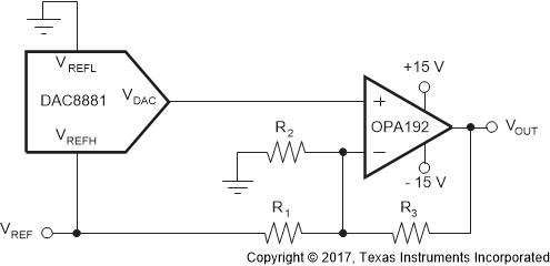
Bipolar Operation Using The DAC8881

The DAC8881 is designed for single-supply operation; however, a bipolar output is also possible using the circuit shown in Figure 72. This circuit gives a bipolar output voltage of VOUT. When GAIN = 1, VOUT can be calculated using Equation 2:
DAC8881 Bipolar_Output_Range.gif
Some pins are omitted for clarity.
Figure 72. Bipolar Operation Using the DAC8881
Equation 2. DAC8881 q_vout3_bas422.gif

Where:

VBIP(CODE) = bipolar output voltage versus CODE from the OPA211.

CODE = 0 to 262143. This is the digital code loaded to the DAC.

VREF = reference high voltage applied to the DAC8881.

As an example, a ±8-V output span can be achieved by using values of 5 V, 6.25 kΩ, 16.67 kΩ, and 10 kΩ for Vref, R1, R2, and R3 respectively.