ZHCSKH5C May 2008 – November 2019 DAC9881
PRODUCTION DATA.
- 1 特性
- 2 应用
- 3 说明
- 4 修订历史记录
- 5 Pin Configuration and Functions
-
6 Specifications
- 6.1 Absolute Maximum Ratings
- 6.2 ESD Ratings
- 6.3 Recommended Operating Conditions
- 6.4 Thermal Information
- 6.5 Electrical Characteristics: AVDD = 5 V
- 6.6 Electrical Characteristics: AVDD = 2.7 V
- 6.7 Timing Requirements—Standalone Operation Without SDO
- 6.8 Timing Requirements—Standalone Operation With SDO and Daisy-Chain Mode
- 6.9 Typical Characteristics: AVDD = 5 V
- 6.10 Typical Characteristics: AVDD = 2.7 V
-
7 Detailed Description
- 7.1 Overview
- 7.2 Functional Block Diagram
- 7.3 Feature Description
- 7.4 Device Functional Modes
- 8 Application and Implementation
- 9 Power Supply Recommendations
- 10Layout
- 11器件和文档支持
- 12机械、封装和可订购信息
封装选项
机械数据 (封装 | 引脚)
- RGE|24
散热焊盘机械数据 (封装 | 引脚)
- RGE|24
订购信息
8.1.1 Bipolar Operation Using the DAC9881
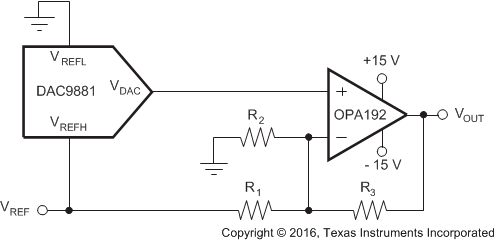
The DAC9881 is designed for single-supply operation; however, a bipolar output is also possible using the circuit shown in Figure 70. This circuit gives a bipolar output voltage of VOUT. When GAIN = 1, VOUT can be calculated using Equation 2:

Some pins are omitted for clarity.
Figure 70. Bipolar Output Range Equation 2. 

where
- VOUT(CODE) = output voltage vs code
- CODE = 0 to 262143. This is the digital code loaded to the DAC
- VREF = reference voltage applied to the DAC9881
As an example, a ±8-V output span can be achieved by using values of 5 V, 6.25 kΩ, 16.67 kΩ, and 10 kΩ for Vref, R1, R2, and R3 respectively.