ZHCSJP7I December 2000 – September 2020 DCP010505B , DCP010505DB , DCP010507DB , DCP010512B , DCP010512DB , DCP010515B , DCP010515DB , DCP011512DB , DCP011515DB , DCP012405B , DCP012415DB
PRODUCTION DATA
- 1 特性
- 2 应用
- 3 说明
- 4 Revision History
- 5 Pin Configuration and Functions
- 6 Specifications
-
7 Detailed Description
- 7.1 Overview
- 7.2 Functional Block Diagrams
- 7.3 Feature Description
- 7.4 Device Functional Modes
-
8 Application and Implementation
- 8.1 Application Information
- 8.2 Typical Application
- 9 Power Supply Recommendations
- 10Layout
- 11Device and Documentation Support
- 12Mechanical, Packaging, and Orderable Information
8.2.5 Decoupling Ceramic Capacitors
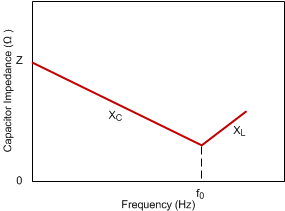
All capacitors have losses because of internal equivalent series resistance (ESR), and to a lesser degree, equivalent series inductance (ESL). Values for ESL are not always easy to obtain. However, some manufacturers provide graphs of frequency versus capacitor impedance. These graphs typically show the capacitor impedance falling as frequency is increased (as shown in Figure 8-4). In Figure 8-4, XC is the reactance due to the capacitance, XL is the reactance due to the ESL, and f0 is the resonant frequency. As the frequency increases, the impedance stops decreasing and begins to rise. The point of minimum impedance indicates the resonant frequency of the capacitor. This frequency is where the components of capacitance and inductance reactance are of equal magnitude. Beyond this point, the capacitor is not effective as a capacitor.
 Figure 8-4 Capacitor Impedance versus Frequency
However, there is a 180° phase difference resulting in cancellation of the imaginary component. The resulting effect is that the impedance at the resonant point is the real part of the complex impedance, namely, the value of the ESR. The output capacitor's resonant frequency must be higher than the default switching frequency (800 kHz) of the device to properly decouple noise at and below the switching frequency.
The effect of the ESR is to cause a voltage drop within the capacitor. The value of this voltage drop is simply the product of the ESR and the transient load current, as shown in Equation 1.
where
- VIN is the voltage at the device input
- VPK is the maximum value of the voltage on the capacitor during charge
- ITR is the transient load current
The other factor that affects the performance is the value of the capacitance. However, for the input and the full wave outputs (single-output voltage devices), ESR is the dominant factor.