ZHCSG81 April 2017 DCPA10505 , DCPA10505D , DCPA10512 , DCPA10512D , DCPA10515 , DCPA10515D
PRODUCTION DATA.
- 1 特性
- 2 应用
- 3 说明
- 4 修订历史记录
- 5 Pin Configuration and Functions
-
6 Specifications
- 6.1 Absolute Maximum Ratings
- 6.2 ESD Ratings
- 6.3 Recommended Operating Conditions
- 6.4 Electrical Characteristics
- 6.5 Switching Characteristics
- 6.6 Typical Characteristics (DCPA10505)
- 6.7 Typical Characteristics (DCPA10512)
- 6.8 Typical Characteristics (DCPA10515)
- 6.9 Typical Characteristics (DCPA10505D)
- 6.10 Typical Characteristics (DCPA10512D)
- 6.11 Typical Characteristics (DCPA10515D)
-
7 Detailed Description
- 7.1 Overview
- 7.2 Functional Block Diagrams
- 7.3 Feature Description
- 8 Application and Implementation
- 9 Power Supply Recommendations
- 10Layout
- 11器件和文档支持
- 12机械、封装和可订购信息
7 Detailed Description
7.1 Overview
The DCPA1 offers up to 1 W of isolated, unregulated output power from a 5-V input source with a typical efficiency of up to 87%. This efficiency is achieved through highly integrated packaging technology and the implementation of a custom power stage and control device. The DCPA1 devices are specified for operational isolation only. The circuit design uses an advanced BiCMOS and DMOS process.
7.2 Functional Block Diagrams
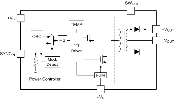
 Figure 31. Single Output Device
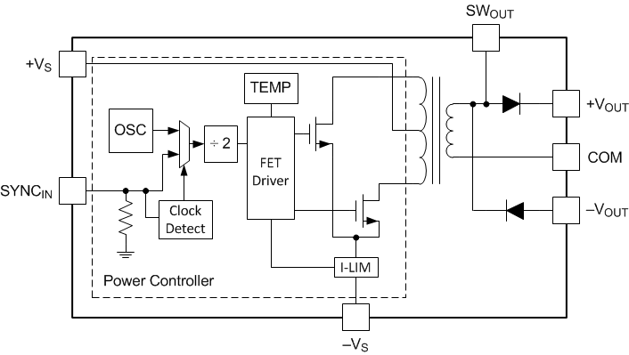
 Figure 32. Dual Output Device
7.3 Feature Description
7.3.1 Isolation
Underwriters Laboratories, UL™ defines several classes of isolation that are used in modern power supplies.
Safety extra low voltage (SELV) is defined by UL (UL1950 E199929) as a secondary circuit which is so designated and protected that under normal and single fault conditions the voltage between any two accessible parts, or between an accessible part and the equipment earthing terminal for operational isolation does not exceed steady state 42 V peak or 60 VDC for more than 1 second.
7.3.1.1 Operation or Functional Isolation
Operational or functional isolation is defined by the use of a high-potential (hipot) test only. Typically, this isolation is defined as the use of insulated wire in the construction of the transformer as the primary isolation barrier. The hipot one-second duration test (dielectric voltage, withstand test) is a production test used to verify that the isolation barrier is functioning. Products with operational isolation should never be used as an element in a safety-isolation system.
7.3.1.2 Basic or Enhanced Isolation
Basic or enhanced isolation is defined by specified creepage and clearance limits between the primary and secondary circuits of the power supply. Basic isolation is the use of an isolation barrier in addition to the insulated wire in the construction of the transformer. Input and output circuits must also be physically separated by specified distances.
7.3.1.3 Continuous Voltage
For a device that has no specific safety agency approvals (operational isolation), the continuous voltage that can be applied across the part in normal operation is less than 42.4 VRMS, or 60 VDC. Ensure that both input and output voltages maintain normal SELV limits. The isolation test voltage represents a measure of immunity to transient voltages.
WARNING
Do not use the device as an element of a safety isolation system that exceeds the SELV limit.
If the device is expected to function correctly with more than 42.4 VRMS or 60 VDC applied continuously across the isolation barrier, then the circuitry on both sides of the barrier must be regarded as operating at an unsafe voltage, and further isolation or insulation systems must form a barrier between these circuits and any user-accessible circuitry according to safety standard requirements.
7.3.1.4 Isolation Voltage
The terms Hipot test, flash-tested, withstand voltage, proof voltage, dielectric withstand voltage, and isolation test voltage all describe the same spec. The terms describe a test voltage applied for a specified time across a component designed to provide electrical isolation to verify the integrity of that isolation. TI’s DCPA1 series of dc-dc converters are all 100% production tested at 1.5 kVAC for one second.
7.3.1.5 Repeated High-Voltage Isolation Testing
Repeated high-voltage isolation testing of a barrier component can degrade the isolation capability, depending on materials, construction, and environment. The DCPA1 series of dc-dc converters have toroidal, enameled, wire isolation transformers with no additional insulation between the primary and secondary windings. While a device can be expected to withstand several times the stated test voltage, the isolation capability depends on the wire insulation. Any material, including this enamel (typically polyurethane), is susceptible to eventual chemical degradation when subject to very-high applied voltages. Therefore, strictly limit the number of high-voltage tests and repeated high-voltage isolation testing. However, if it is absolutely required, reduce the voltage by 20% from specified test voltage with a duration limit of one second per test.
7.3.2 Power Stage
The DCPA1 series of devices uses a push-pull, center-tapped topology. The DCPA1 devices switch at 425 kHz (divide-by-2 from an 850-kHz oscillator).
7.3.3 Input and Output Capacitors
For all DCPA1 designs, a minimum 2.2-μF, low-ESR, ceramic input capacitor is required. Place the input capacitor as close as possible to the device input pins, +VS and –VS, to ensure good startup performance.
The recommended typical output capacitance for each output of any DCPA1 device is 1.0-μF of low-ESR, ceramic capacitance. Adding additional output capacitance will aid in ripple reduction, however, any additional capacitance will also require additional input current at start-up.
7.3.4 Oscillator And Watchdog Circuit
The onboard, 850-kHz oscillator generates the switching frequency via a divide-by-2 circuit. The oscillator can be synchronized to an external source, and is used to minimize system noise. A watchdog circuit checks the operation of the oscillator circuit.
7.3.5 Synchronization
When more than one DC/DC converter is needed onboard, beat frequencies and other electrical interference can be generated. This interference occurs because of the small variations in switching frequencies between the DC/DC converters.
The DCPA1 series of devices overcomes this interference by allowing devices to synchronize to an external clock. The SYNCIN pin responds to the rising edge of the external clock. If the external clock is removed, the DCPA1 will return to the frequency of the internal oscillator. If unused, it is recommended to connect this pin to the input side common, –VS.
7.3.6 SWOUT
The SWOUT pin is directly connected to one winding of the transformer secondary prior to the output rectifier. It is not recommended to pull current from this pin. Do not connect capacitance directly to this pin as it will degrade performance. The SWOUT pin is not compatible with the SYNCIN pin, therefore these two pins should not be connected together.
7.3.7 Soft Start
The DCPA1 series of devices includes a soft-start feature that prevents high in-rush current during power up. Once input power is applied, there is a delay of typically 10 ms before the output voltage begins to rise. Once the output voltage begins to rise, the soft start time is typically 5 ms.
7.3.8 Load Regulation
The load regulation of the DCPA1 series of devices is specified at 10% to 100% load. Operation below 10% load may cause the output voltage to increase up to 40% higher than the typical output voltage. Placing a minimum 10% load will ensure the output voltage is within the range specified in the Electrical Characteristics table.
7.3.9 Thermal Performance
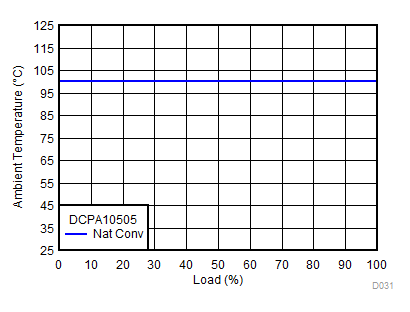
The DCPA1 family of devices have been characterized to operate over an ambient temperature range of –40°C to +100°C. The Safe Operating Area curve shown below in Figure 33, represents the operating conditions of the DCPA1 devices where the maximum thermal ratings will not be exceeded. Figure 33 shows that all DCPA1 devices can safely operate over the full ambient temperature range, without airflow, to the full current rating of the device.
 Figure 33. Thermal Safe Operating Area
7.3.9.1 Thermal Protection
The DCPA1 series of devices are protected by a thermal-shutdown circuit.
If the on-chip temperature rises above 150°C, the device shuts down. Normal operation resumes as soon as the temperature falls below 150°C. While the overtemperature condition continues, operation randomly cycles on and off. This cycling continues until the temperature is reduced.
7.3.10 Current Limit
For protection against a short circuit on the output, the DCPA1 series of devices have a built in current limit protection threshold of 1.75A (typical). These devices are not intended to be used at output currents greater than the device's output current rating as shown in the Electrical Characteristics table. Operating at currents greater than the device's current rating, but less than current limit threshold will cause excessive stress to the internal components. For protection against a partial short circuit condition, an input fuse or output fuse is recommended.
7.3.11 Construction
The basic construction of the DCPA1 series of devices is the same as standard integrated circuits. The molded package contains no substrate. The DCPA1 series of devices are constructed using an IC, rectifier diodes, and a wound magnetic toroid on a leadframe. Because the package contains no solder, the devices do not require any special printed circuit board (PCB) assembly processing. This architecture results in an isolated DC/DC converter with inherently high reliability.