SBAS368D May 2006 – December 2016 DDC264
PRODUCTION DATA.
- 1 Features
- 2 Applications
- 3 Description
- 4 Revision History
- 5 Device Comparison Table
- 6 Pin Configuration and Functions
- 7 Specifications
-
8 Detailed Description
- 8.1 Overview
- 8.2 Functional Block Diagram
- 8.3
Feature Description
- 8.3.1 Dual Switched Integrator: Basic Integration Cycle
- 8.3.2 Integration Capacitors
- 8.3.3 Voltage Reference
- 8.3.4 Serial Data Output and Control Interface
- 8.4 Device Functional Modes
- 8.5 Programming
- 8.6 Register Maps
- 9 Application and Implementation
- 10Power Supply Recommendations
- 11Layout
- 12Device and Documentation Support
- 13Mechanical, Packaging, and Orderable Information
11 Layout
11.1 Layout Guidelines
11.1.1 Shielding Analog Signal Paths
As with any precision circuit, careful PCB layout ensures the best performance. It is essential to make short, direct interconnections and avoid stray wiring capacitance—particularly at the analog input pins and QGND. The analog input pins are low-impedance and extremely sensitive to extraneous noise. The QGND pin must be treated as a sensitive analog signal and connected directly to the supply ground with proper shielding. Leakage currents between the PCB traces can exceed the input bias current of the DDC264 if shielding (guard) is not implemented. Digital signals (including digital supply) must be kept as far as possible from the analog input signals on the PCB. If possible, avoid running digital supply planes over analog ground or signals.
11.1.2 Power Supply Routing
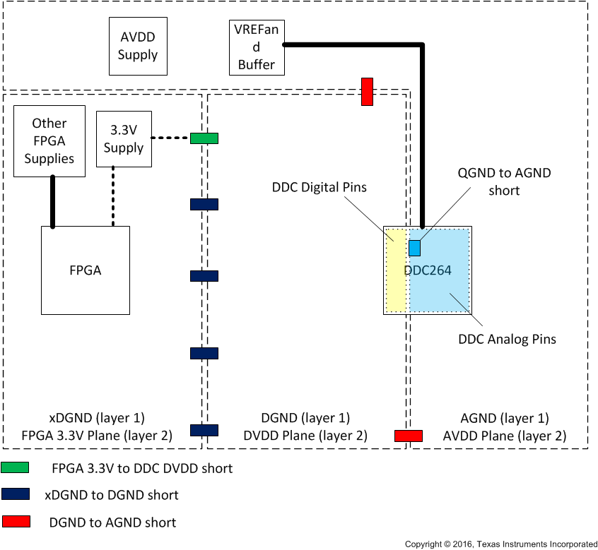
Figure 36 shows a diagram summarizing the concept behind the power supply distribution used in the DDC264 evaluation module (EVM).
In theoretical terms, from an isolation perspective, generating all required supplies from different sources (LDOs) may be the best but may actually be not practical/too costly. In Figure 36, an analog supply is used to generate and drive the VREF/Buffer supplies and the DDC AVDD. The AGND runs parallel to this plane (above or below). The VREF signal is also routed in the same location. As seen on the figure, these do not overlap with the digital supply/ground/signals at any moment.
Away from the analog portion, a digital supply can be used/shared between the FPGA and the DDC. Nevertheless a star configuration is used to isolate the effect between both as much as possible. For the same reason, the physical planes of both digital supplies are also separated.
Notice nevertheless, that it is not a bad practice to include places along the separation between all these planes to allow for shorts, whether through a zero value resistor or a ferrite bead. This enables fine tuning of the design performance.
11.1.3 Reference Routing
In the case where only one reference buffer is used for multiple DDCs, all reference pins must be as isolated as possible from each other to avoid interactions between devices. One potential approach to this is to do a star connection where the traces to the reference of each device are connected to the others only at the output of the driver. Keep VREF shielded from any noisy signals, like digital traces or supplies.
11.2 Layout Example
 Figure 36. DDC264 Layout Example