ZHCSFA7A July 2016 – April 2017 DIX4192-Q1
PRODUCTION DATA.
- 1 特性
- 2 应用
- 3 说明
- 4 修订历史记录
- 5 说明 (续)
- 6 Device Comparison Table
- 7 Pin Configuration and Functions
- 8 Specifications
-
9 Detailed Description
- 9.1 Overview
- 9.2 Functional Block Diagram
- 9.3
Feature Description
- 9.3.1 RESET Operation
- 9.3.2 Master and Reference Clocks
- 9.3.3 Audio Serial Port Operation
- 9.3.4 Overview of the AES3 Digital Audio Interface Protocol
- 9.3.5 Digital Interface Transmitter (DIT) Operation
- 9.3.6 Digital Interface Receiver (DIR) Operation
- 9.3.7 General-Purpose Digital Outputs
- 9.3.8 Interrupt Output
- 9.4 Device Functional Modes
- 9.5 Register Maps
- 10Application and Implementation
- 11Power Supply Recommendations
- 12Layout
- 13器件和文档支持
- 14机械、封装和可订购信息
10 Application and Implementation
NOTE
Information in the following applications sections is not part of the TI component specification, and TI does not warrant its accuracy or completeness. TI’s customers are responsible for determining suitability of components for their purposes. Customers should validate and test their design implementation to confirm system functionality.
10.1 Application Information
Typical application diagrams and power-supply connections are presented in this section to aid the customer in hardware designs employing the DIX4192-Q1 device.
Figure 69 shows typical application connections for the DIX4192-Q1 using an SPI host interface. The SPI host will typically be a microcontroller, digital signal processor, or programmable logic device. In addition to providing the SPI bus master, the host may be used to process interrupt and flag outputs from the DIX4192-Q1. The audio serial ports are connected to external digital audio devices, which may include data converters, digital signal processors, digital audio interface receivers or transmitters, or other logic devices. The DIR inputs and DIT outputs are connected to line, optical, or logic interfaces (see Receiver Input Interfacing and Transmitter Output Interfacing). Master and DIR reference clock sources are also shown.
Figure 70 shows typical application connections for the DIX4192-Q1 using an I2C bus interface. The I2C bus master will typically be a microcontroller, digital signal processor, or programmable logic device. In addition to providing the I2C bus master, the host may be used to process interrupt and flag outputs from the DIX4192-Q1. Pullup resistors are connected from SCL (pin 20) and SDA (pin 22) to the VIO supply rail. These resistors are required for the open drain outputs of the I2C interface. All other connections to the DIX4192-Q1 are the same as the SPI host case discussed previously.
Figure 71 shows the recommended power-supply connections and bypassing for the DIX4192-Q1. In this case, it is assumed that the VIO, VDD33, and VCC supplies are powered from the same 3.3-V power source. The VDD18 core supply is powered from a separate supply, or derived from the 3.3-V supply using a linear voltage regulator, as shown with the optional regulator circuitry of Figure 71.
The 0.1-μF bypass capacitors are surface-mount X7R ceramic, and must be located as close to the device as possible. These capacitors must be connected directly between the supply and corresponding ground pins of the DIX4192-Q1. The ground pin is then connected directly to the ground plane of the printed circuit board (PCB). The larger value capacitors, shown connected in parallel to the 0.1-μF capacitors, are recommended. At a minimum, there must at least be footprints on the PCB for installation of these larger capacitors, so that experiments can be run with and without the capacitors installed, in order to determine the effect on the measured performance of the DIX4192-Q1. The larger value capacitors can be surface-mount X7R multilayer ceramic or tantalum chip.
The substrate ground, BGND (pin 44), must be connected by a PCB trace to AGND (pin 10). The AGND pin is then connected directly to the ground plane. This connection helps to reduce noise in the DIR section of the device, aiding the overall jitter and noise tolerance for the receiver.
A series resistor is shown between the 3.3-V supply and VCC (pin 9) connection. This resistor combines with the bypass capacitors to create a simple RC filter to remove higher frequency components from the VCC supply. The series resistor must be a metal film type for best filtering characteristics. As a substitute for the resistor, a ferrite bead can be used, although it may have to be physically large in order to contribute to the filtering.
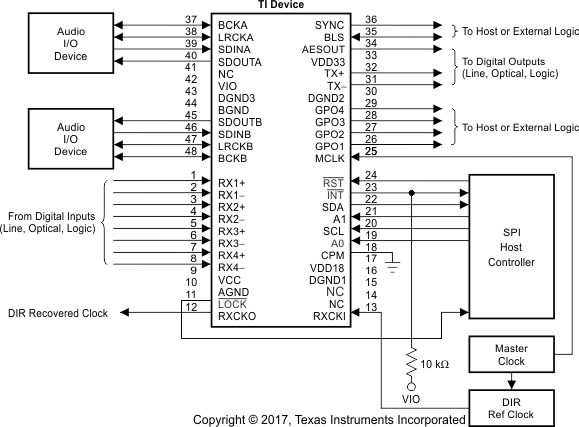 Figure 69. Typical Application Diagram Using SPI Host Interface
(See Figure 71 for Power-Supply Connections)
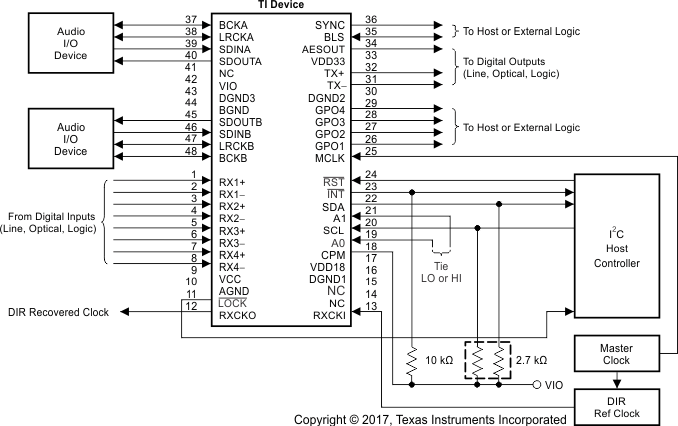 Figure 70. Typical Application Diagram Using I2C Host Interface
(See Figure 71 for Power-Supply Connections)
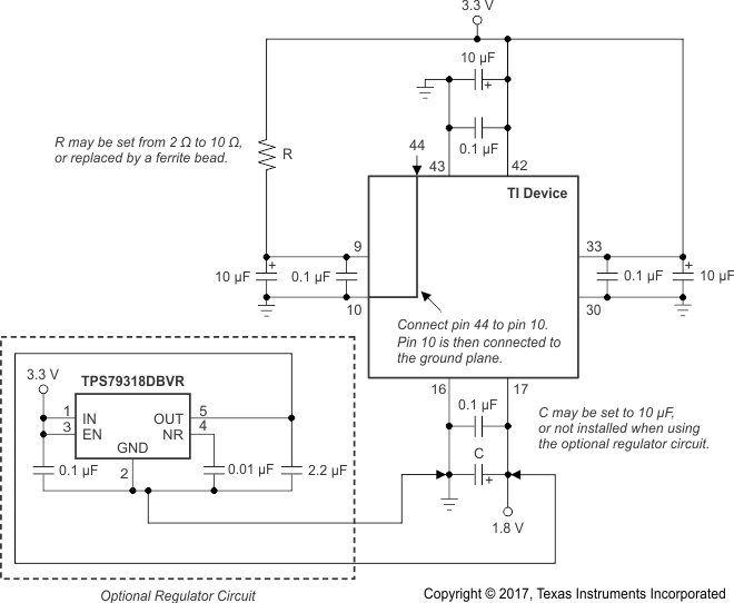 Figure 71. Recommended Power-Supply Connections
10.1.1 Digital Audio Transformer Vendors
Transformers are shown in this data sheet for both receiver and transmitter balanced and unbalanced line interface implementations. For the Texas Instruments Pro Audio evaluation modules, transformers from Scientific Conversion are used. In addition to Scientific Conversion, there are other vendors that offer transformer products for digital audio interface applications. Please refer to the following manufacturer websites for details regarding their products and services. Other transformer vendors may also be available by searching catalog and/or Internet resources.
- Scientific Conversion: http://scientificonversion.com
- Schott Corporation: http://schottcorp.com
- Pulse Engineering: http://pulseeng.com
10.1.2 Receiver Input Interfacing
This section details the recommended interfaces for the DIX4192-Q1 line receiver inputs. Balanced and unbalanced line interfaces, in addition to optical receiver and external logic interfacing, are discussed.
For professional digital audio interfaces, 110-Ω balanced line interfaces are either required or preferred. Transformer coupling is commonly employed to provide isolation and to improve common-mode noise rejection. Figure 72 shows the recommended transformer-coupled balanced line receiver interface for the DIX4192-Q1. The transformer is specified for a 1:1 turn ratio, and must exhibit low inter-winding capacitance for best performance. Due to the DC bias on the line receiver inputs, 0.1-μF capacitors are used for AC-coupling the transformer to the line receiver inputs. On the line side of the transformer, an optional 0.1-μF capacitor is shown for cases where a DC bias may be applied at the transmitter side of the connection. The coupling capacitors must be surface-mount ceramic chip type with an X7R or C0G dielectric.
 Figure 72. Transformer-Coupled Balanced Input Interface
Unbalanced 75-Ω coaxial cable interfaces are commonly employed in consumer and broadcast audio applications. Designs with and without transformer line coupling may be used. Figure 73(a) shows the recommended 75-Ω transformer-coupled line interface, which shares many similarities to the balanced design shown in Figure 72. Once again, the transformer provides isolation and improved noise rejection. Figure 73(b) shows the transformer-free interface, which is commonly used for S/PDIF consumer connections.
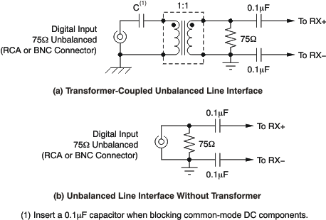 Figure 73. Unbalanced Line Input Interfaces
Optical interfaces using all-plastic fiber are commonly employed for consumer audio equipment where interconnections are less than 10 m in length. Optical receiver modules used for a digital audio interface operate from either a single 3.3-V or 5-V supply and have a TTL–, CMOS-, or low-voltage CMOS-compatible logic output. Interfacing to 3.3-V optical receivers is straightforward when the optical receiver supply is powered from the DIX4192-Q1 VDD33 power source, as shown in Figure 74. For the 5-V optical receivers, the output high logic level may exceed the DIX4192-Q1 line receiver absolute maximum input voltage. A level translator is required, placed between the optical receiver output and the DIX4192-Q1 line receiver input. Figure 75 shows the recommended input circuit when interfacing a 5-V optical receiver to the DIX4192-Q1 line receiver inputs. The Texas Instruments SN74LVC1G125 single buffer IC is operated from the same 3.3-V supply used for DIX4192-Q1 VDD33 supply. This buffer includes a 5-V tolerant digital input, and provides the logic level translation required for the interface.
 Figure 74. Interfacing to a 3.3-V Optical Receiver Module
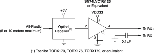 Figure 75. Interfacing to a 5-V Optical Receiver Module
The DIX4192-Q1 line receivers may also be driven directly from external logic or line receiver devices with TTL or CMOS outputs. If the logic driving the line receiver is operated from 3.3 V, then logic level translation will not be required. However, if the external logic is operated from a power-supply voltage that exceeds the maximum VDD33 supply voltage of the DIX4192-Q1, or operates from a supply voltage lower than 3.3 V, then level translation is required. Figure 76 shows the recommended logic level translation methods, using buffers and level translators available from Texas Instruments.
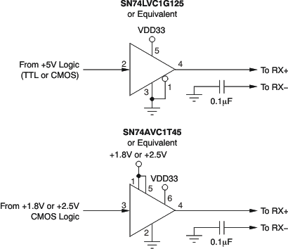 Figure 76. CMOS and TTL Input Logic Interface
10.1.3 Transmitter Output Interfacing
This section details the recommended interfaces for the DIX4192-Q1 transmitter line driver and CMOS-buffered outputs. Balanced and unbalanced line interfaces, in addition to optical transmitter and external logic interfacing, will be discussed.
For professional digital audio interfaces, 110-Ω balanced line interfaces are either required or preferred. Transformer coupling is commonly employed to provide isolation and to improve common-mode noise performance. Figure 77 shows the recommended transformer-coupled balanced line driver interface for the DIX4192-Q1. The transformer is specified for a 1:1 turn ratio, and must exhibit low inter-winding capacitance for best performance. To eliminate residual DC bias, a 0.1-μF capacitor is used for AC-coupling the transformer to the line driver outputs. The coupling capacitor must be a surface-mount ceramic chip type with an X7R or C0G dielectric.
 Figure 77. Transformer-Coupled Balanced Output Interface
Unbalanced 75-Ω coaxial cable interfaces are commonly employed in consumer and broadcast audio applications. Designs with and without transformer line coupling may be used. Figure 78(a) shows the recommended 75-Ω transformer-coupled line driver interface, which shares many similarities to the balanced design shown in Figure 77. Figure 78(b) shows the transformer-free line driver interface, which is commonly used for S/PDIF consumer connections.
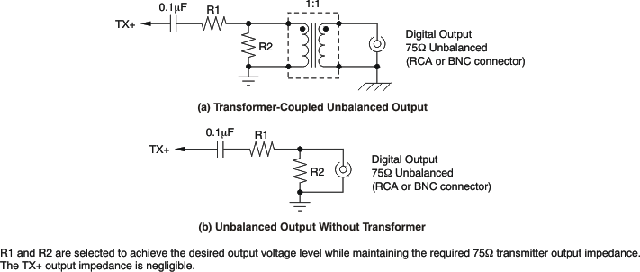 Figure 78. Unbalanced Line Output Interfaces
Optical interfaces using all-plastic fiber are commonly employed for consumer audio equipment where interconnections are less than 10 m in length. Most optical transmitter modules used for a digital audio interface operate from a single 3.3-V or 5-V supply and have a TTL-compatible logic input. The CMOS-buffered transmitter output of the DIX4192-Q1, AESOUT (pin 34), is capable of driving the optical transmitter with VIO supply voltages down to 3 V. If the VIO supply voltage is less than 3 V, then level translation logic is required to drive the optical transmitter input. A good choice for this application is the Texas Instruments SN74AVC1T45 single bus transceiver. This device features two power-supply rails, one for the input side and one for the output side. For this application, the input side supply is powered from the VIO supply, while the output side is powered from a 3.3-V supply. This configuration will boost the logic high level to a voltage suitable for driving the TTL-compatible input configuration. Figure 79 shows the recommended optical transmitter interface circuits.
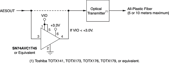 Figure 79. Interfacing to an Optical Transmitter Module
The AESOUT output may also be used to drive external logic or line driver devices directly. Figure 80 shows the recommended logic interface techniques, including connections with and without level translation. Figure 81 shows an external line driver interface using the Texas Instruments SN75ALS191 dual differential line driver. If the VIO supply of the DIX4192-Q1 is set from 3 V to 3.3 V, no logic level translation will be required between the AESOUT output and the line driver input. If the VIO supply voltage is below this range, then the optional logic level translation logic of Figure 81 will be required. The SN75ALS191 dual line driver is especially useful in applications where simultaneous 75-Ω and 110-Ω line interfaces are required.
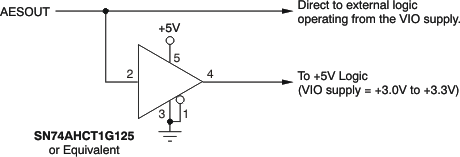 Figure 80. CMOS or TTL Output Logic Interface
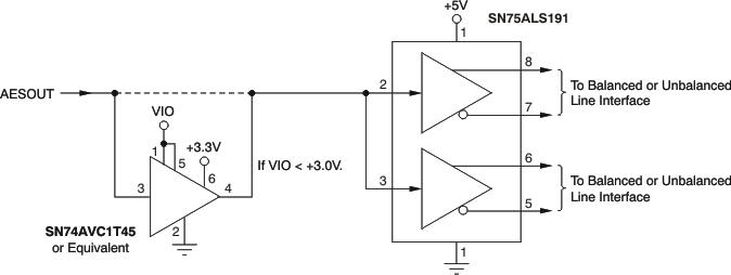 Figure 81. External Line Driver Interface
10.2 Typical Application
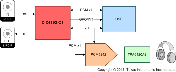 Figure 82. DIX4192-Q1 Typical Application
10.2.1 Design Requirements
For this design example, use the parameters listed in Table 39.
Table 39. Design Parameters
| DESIGN PARAMETER | EXAMPLE VALUE |
|---|---|
| Audio input | PCM x2, differential S and PDIF x4 |
| Audio output | PCM x2, S and PDIF x4 |
| Control | Host 12C |
| RXCKI or MCLK | 24.576 MHz |
10.2.2 Detailed Design Procedure
10.2.2.1 Differential Line Inputs and Output
The DIX4192-Q1 has a total of 4 differential Line inputs and one Differential Line output. The 4 inputs are MUXed to one port for decoding and the audio data is sent to the internal bus of the device. The differential line output can choose from either the AES3 encoder or directly from one of the RX inputs. The AES3 encoder can encode either of the serial ports or the DIR itself. User data and channel status data can be updated in registers.
10.2.2.2 Serial Ports
The DIX4192-Q1 has two serial ports which each support both input and output of PCM data. This allows a device to receive data from one of the serial ports and then return audio to the DIX4192-Q1 to be routed to another output of the DIX4192-Q1. For example in this application the DSP can receive audio from the DIX4192-Q1 that was input to the DIX4192-Q1 over S/PDIF, then after processing the DSP can send audio back the DIX4192-Q1 over the same serial port. This processed audio can then be sent back out the S/PDIF transmit port of the DIX4192-Q1 or to the PCM5242 DAC on the other serial port.
10.2.3 Application Curves
