ZHCSP43C november 2021 – july 2023 DLP160AP
PRODUCTION DATA
- 1
- 1 特性
- 2 应用
- 3 说明
- 4 Revision History
- 5 Pin Configuration and Functions
-
6 Specifications
- 6.1 Absolute Maximum Ratings
- 6.2 Storage Conditions
- 6.3 ESD Ratings
- 6.4 Recommended Operating Conditions
- 6.5 Thermal Information
- 6.6 Electrical Characteristics
- 6.7 Timing Requirements
- 6.8 Switching Characteristics
- 6.9 System Mounting Interface Loads
- 6.10 Micromirror Array Physical Characteristics
- 6.11 Micromirror Array Optical Characteristics
- 6.12 Window Characteristics
- 6.13 Chipset Component Usage Specification
- 7 Detailed Description
- 8 Application and Implementation
- 9 Power Supply Recommendations
- 10Layout
- 11Device and Documentation Support
- 12Mechanical, Packaging, and Orderable Information
6.10 Micromirror Array Physical Characteristics
| PARAMETER | VALUE | UNIT | ||||
|---|---|---|---|---|---|---|
| Number of active columns | See Figure 6-15 | 640(2) | micromirrors | |||
| Number of active rows | See Figure 6-15 | 360(2) | micromirrors | |||
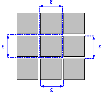
| Micromirror (pixel) pitch | See Figure 6-16 | 5.4 | µm | |||
| Micromirror active array width | Micromirror pitch × number of active columns; see Figure 6-15 | 3.456 | mm | |||
| Micromirror active array height | Micromirror pitch × number of active rows; see Figure 6-15 | 1.944 | mm | |||
| Micromirror active border | Pond of micromirror (POM)(1) | 20 | micromirrors/side | |||
(1) The structure and qualities of the border around the active array include a band of partially functional micromirrors called the POM. These micromirrors are structurally or electrically prevented from tilting toward the bright or ON state, but still require an electrical bias to tilt toward OFF.
(2) The
DLP image processing in the DMD combined with limited input resolution for this
chipset result in a 320 x 180 image resolution being displayed.
 Figure 6-15 Micromirror Array Physical Characteristics
 Figure 6-16 Mirror (Pixel) Pitch