ZHCSP44D October 2021 – October 2024 DLP160CP
PRODUCTION DATA
- 1
- 1 特性
- 2 应用
- 3 说明
- 4 Pin Configuration and Functions
-
5 Specifications
- 5.1 Absolute Maximum Ratings
- 5.2 Storage Conditions
- 5.3 ESD Ratings
- 5.4 Recommended Operating Conditions
- 5.5 Thermal Information
- 5.6 Electrical Characteristics
- 5.7 Timing Requirements
- 5.8 Switching Characteristics
- 5.9 System Mounting Interface Loads
- 5.10 Micromirror Array Physical Characteristics
- 5.11 Micromirror Array Optical Characteristics
- 5.12 Window Characteristics
- 5.13 Chipset Component Usage Specification
- 6 Detailed Description
- 7 Application and Implementation
- 8 Power Supply Recommendations
- 9 Layout
- 10Device and Documentation Support
- 11Revision History
- 12Mechanical, Packaging, and Orderable Information
5.7 Timing Requirements
Device electrical characteristics are over Recommended Operating Conditions unless otherwise noted.
| MIN | NOM | MAX | UNIT | |||
|---|---|---|---|---|---|---|
| LPSDR | ||||||
| tr | Rise slew rate(1) | (30% to 80%) × VDD, Figure 5-3 | 1 | 3 | V/ns | |
| tƒ | Fall slew rate(1) | (70% to 20%) × VDD, Figure 5-3 | 1 | 3 | V/ns | |
| tr | Rise slew rate(2) | (20% to 80%) × VDD, Figure 5-3 | 0.25 | V/ns | ||
| tƒ | Fall slew rate(2) | (80% to 20%) × VDD, Figure 5-3 | 0.25 | V/ns | ||
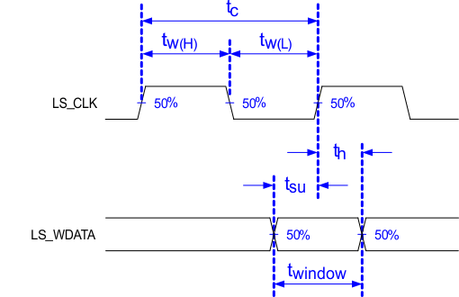
| tc | Cycle time LS_CLK | Figure 5-2 | 7.7 | 8.3 | ns | |
| tW(H) | Pulse duration LS_CLK high | 50% to 50% reference points, Figure 5-2 | 3.1 | ns | ||
| tW(L) | Pulse duration LS_CLK low | 50% to 50% reference points, Figure 5-2 | 3.1 | ns | ||
| tsu | Setup time | LS_WDATA valid before LS_CLK ↑, Figure 5-2 | 1.5 | ns | ||
| th | Hold time | LS_WDATA valid after LS_CLK ↑, Figure 5-2 | 1.5 | ns | ||
| tWINDOW | Window time(1) (3) | Setup time + hold time, Figure 5-2 | 3 | ns | ||
| tDERATING | Window time derating(1) (3) | For each 0.25V/ns reduction in slew rate below 1V/ns, Figure 5-5 | 0.35 | ns | ||
| SubLVDS | ||||||
| tr | Rise slew rate | 20% to 80% reference points, Figure 5-4 | 0.7 | 1 | V/ns | |
| tƒ | Fall slew rate | 80% to 20% reference points, Figure 5-4 | 0.7 | 1 | V/ns | |
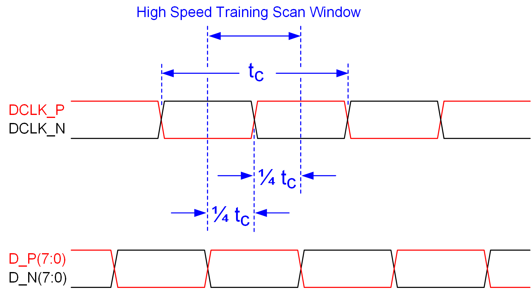
| tc | Cycle time DCLK | Figure 5-6 | 1.79 | 1.85 | ns | |
| tW(H) | Pulse duration DCLK high | 50% to 50% reference points, Figure 5-6 | 0.79 | ns | ||
| tW(L) | Pulse duration DCLK low | 50% to 50% reference points, Figure 5-6 | 0.79 | ns | ||
| tsu | Setup time | D(0:7) valid before DCLK ↑ or DCLK ↓, Figure 5-6 | Setup and Hold times are defined by tWINDOW | |||
| th | Hold time | D(0:7) valid after DCLK ↑ or DCLK ↓, Figure 5-6 | Setup and Hold times are defined by tWINDOW | |||
| tWINDOW | Window time | Setup time + hold time, Figure 5-6, Figure 5-7 | 0.3 | ns | ||
| tLVDS-ENABLE+REFGEN | Power-up receiver(4) | 2000 | ns | |||
(1) Specification is for LS_CLK and LS_WDATA pins. Refer to LPSDR input rise slew rate and fall slew rate in Figure 5-3.
(2) Specification is for DMD_DEN_ARSTZ pin. Refer to LPSDR input rise and fall slew rate in Figure 5-3.
(3) Window time derating example: 0.5V/ns slew rate increases the window time by 0.7ns, from 3ns to 3.7ns.
(4) Specification is for SubLVDS receiver time only and does not take into account commanding and latency after commanding.
Low-speed interface is LPSDR and adheres to the Section 5.6 and AC/DC Operating Conditions table in JEDEC Standard No. 209B, Low Power Double Data Rate (LPDDR) JESD209B.
Figure 5-2 LPSDR Switching Parameters Figure 5-3 LPSDR Input Rise and Fall Slew Rate
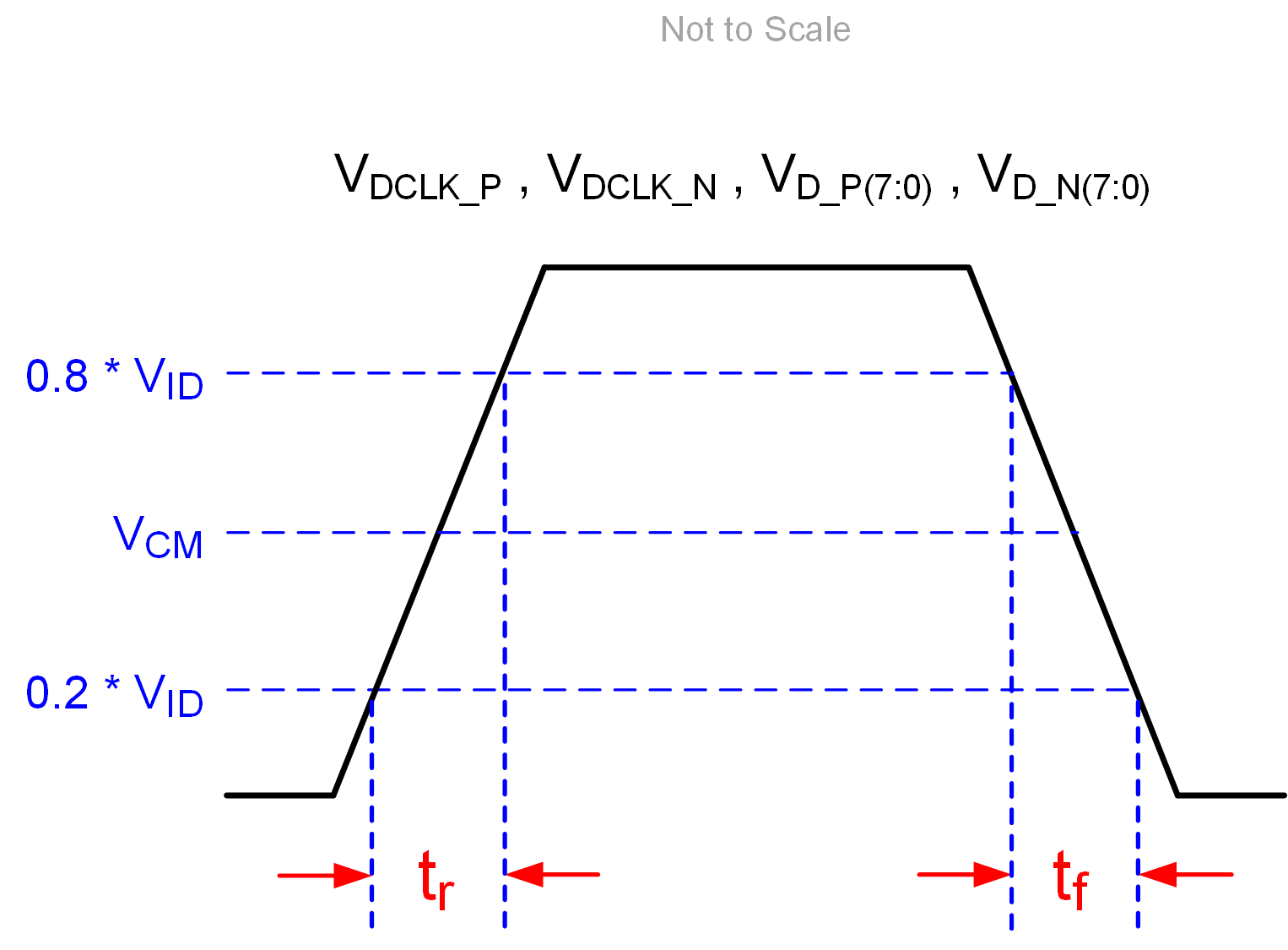 Figure 5-4 SubLVDS Input Rise and Fall Slew Rate
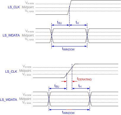 Figure 5-5 Window Time Derating Concept
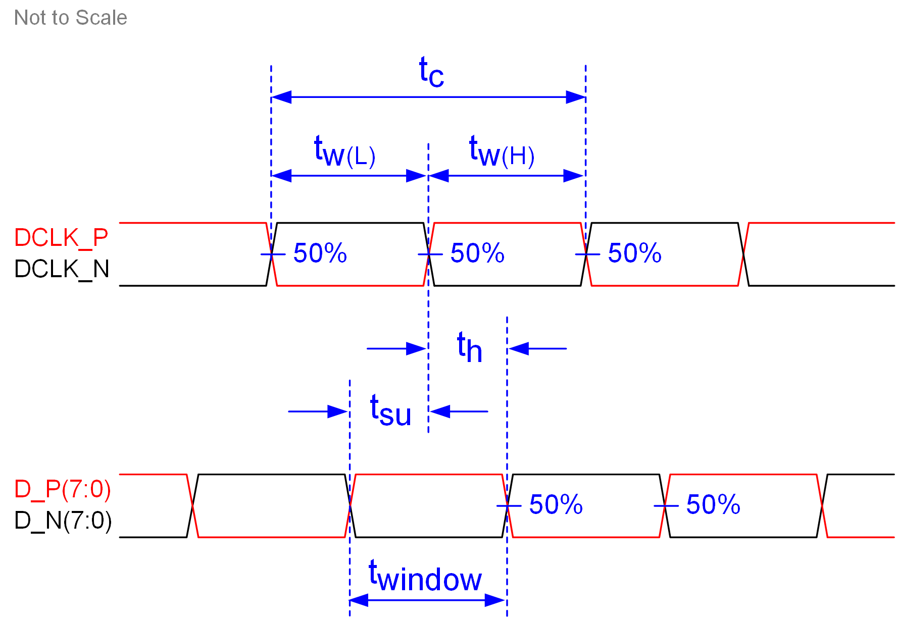 Figure 5-6 SubLVDS Switching Parameters
 Figure 5-8 SubLVDS Voltage Parameters
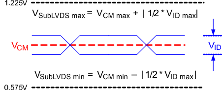 Figure 5-9 SubLVDS Waveform Parameters
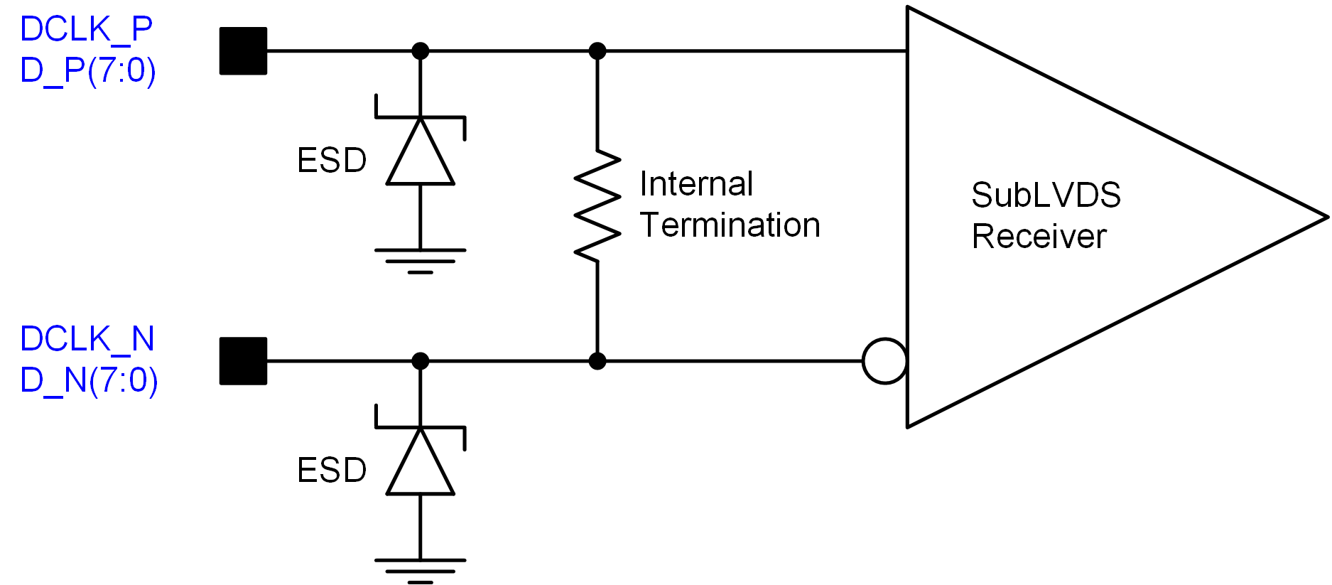 Figure 5-10 SubLVDS Equivalent Input Circuit
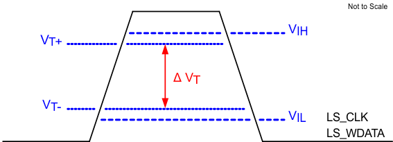 Figure 5-11 LPSDR Input Hysteresis
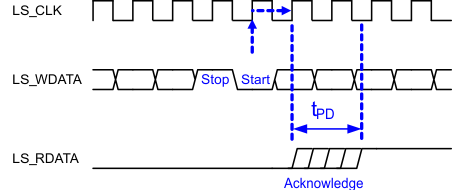 Figure 5-12 LPSDR Read Out
See Section 6.3.4 for more information.
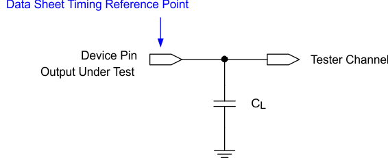
Figure 5-13 Test Load Circuit for Output Propagation Measurement