ZHCSOH3B July 2021 – May 2022 DLP300S
PRODUCTION DATA
- 1 特性
- 2 应用
- 3 说明
- 4 Revision History
- 5 Pin Configuration and Functions
-
6 Specifications
- 6.1 Absolute Maximum Ratings
- 6.2 Storage Conditions
- 6.3 ESD Ratings
- 6.4 Recommended Operating Conditions
- 6.5 Thermal Information
- 6.6 Electrical Characteristics
- 6.7 Timing Requirements
- 6.8 Switching Characteristics
- 6.9 System Mounting Interface Loads
- 6.10 Micromirror Array Physical Characteristics
- 6.11 Micromirror Array Optical Characteristics
- 6.12 Window Characteristics
- 6.13 Chipset Component Usage Specification
- 6.14 Software Requirements
- 7 Detailed Description
- 8 Application and Implementation
- 9 Power Supply Recommendations
- 10Layout
- 11Device and Documentation Support
- 12Mechanical, Packaging, and Orderable Information
7.6 Micromirror Array Temperature Calculation
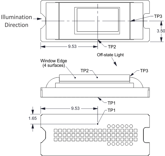
 Figure 7-1 Thermal Test Point Location - FQK Package
Micromirror array temperature cannot be measured directly, therefore it must be computed analytically from measurement points on the outside of the package, the package thermal resistance, the electrical power, and the illumination heat load. The relationship between array temperature and the reference ceramic temperature shown as TP1 in Figure 7-1 is provided by the following equations:
where
- TARRAY = Computed micromirror array temperature (°C)
- TCERAMIC = Measured ceramic temperature (°C) (TP1 location)
- RARRAY-TO-CERAMIC = Thermal resistance of package specified in Section 6.5 from array to ceramic TP1 (°C/W)
- QARRAY = Total DMD power on the array (electrical + absorbed) (W)
- QELECTRICAL = Nominal electrical power (W)
- QINCIDENT = measured total illumination optical power at DMD (W)
- QILLUMINATION = (QINCIDENT × DMD average thermal absortivity) (W)
- DMD average thermal absortivity = 0.40
The electrical power dissipation of the DMD is variable and depends on the voltages, data rates, and operating frequencies. A nominal electrical power dissipation to use when calculating array temperature is 0.1 W. The absorbed power from the illumination source is variable and depends on the operating state of the micromirrors and the intensity of the light source. The equations shown above are valid for each DMD chip in a system. It assumes illumination distribution of 83.7% on the active array and 16.3% on the area outside the array.