ZHCSOH3B July 2021 – May 2022 DLP300S
PRODUCTION DATA
- 1 特性
- 2 应用
- 3 说明
- 4 Revision History
- 5 Pin Configuration and Functions
-
6 Specifications
- 6.1 Absolute Maximum Ratings
- 6.2 Storage Conditions
- 6.3 ESD Ratings
- 6.4 Recommended Operating Conditions
- 6.5 Thermal Information
- 6.6 Electrical Characteristics
- 6.7 Timing Requirements
- 6.8 Switching Characteristics
- 6.9 System Mounting Interface Loads
- 6.10 Micromirror Array Physical Characteristics
- 6.11 Micromirror Array Optical Characteristics
- 6.12 Window Characteristics
- 6.13 Chipset Component Usage Specification
- 6.14 Software Requirements
- 7 Detailed Description
- 8 Application and Implementation
- 9 Power Supply Recommendations
- 10Layout
- 11Device and Documentation Support
- 12Mechanical, Packaging, and Orderable Information
6.10 Micromirror Array Physical Characteristics
| PARAMETER | VALUE | UNIT | ||
|---|---|---|---|---|
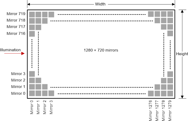
| Number of active columns | See Figure 6-16 | 1280 | micromirrors | |
| Number of active rows | See Figure 6-16 | 720 | micromirrors | |
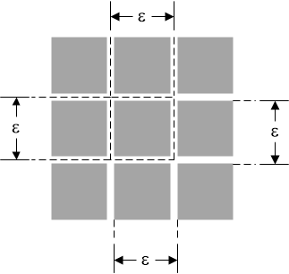
| ε | Micromirror (pixel) pitch | See Figure 6-17 | 5.4 | µm |
| Micromirror active array width | Micromirror pitch × number of active columns; see Figure 6-16 | 6.912 | mm | |
| Micromirror active array height | Micromirror pitch × number of active rows; see Figure 6-16 | 3.888 | mm | |
| Micromirror active border | Pond of micromirror (POM)(1) | 20 | micromirrors/side | |
(1) The structure and qualities of the border around the active array includes a band of partially functional micromirrors called the POM. These micromirrors are structurally and/or electrically prevented from tilting toward the bright or ON state, but still require an electrical bias to tilt toward OFF.
 Figure 6-16 Micromirror Array Physical Characteristics
 Figure 6-17 Mirror
(Pixel) Pitch