ZHCSOH3B July 2021 – May 2022 DLP300S
PRODUCTION DATA
- 1 特性
- 2 应用
- 3 说明
- 4 Revision History
- 5 Pin Configuration and Functions
-
6 Specifications
- 6.1 Absolute Maximum Ratings
- 6.2 Storage Conditions
- 6.3 ESD Ratings
- 6.4 Recommended Operating Conditions
- 6.5 Thermal Information
- 6.6 Electrical Characteristics
- 6.7 Timing Requirements
- 6.8 Switching Characteristics
- 6.9 System Mounting Interface Loads
- 6.10 Micromirror Array Physical Characteristics
- 6.11 Micromirror Array Optical Characteristics
- 6.12 Window Characteristics
- 6.13 Chipset Component Usage Specification
- 6.14 Software Requirements
- 7 Detailed Description
- 8 Application and Implementation
- 9 Power Supply Recommendations
- 10Layout
- 11Device and Documentation Support
- 12Mechanical, Packaging, and Orderable Information
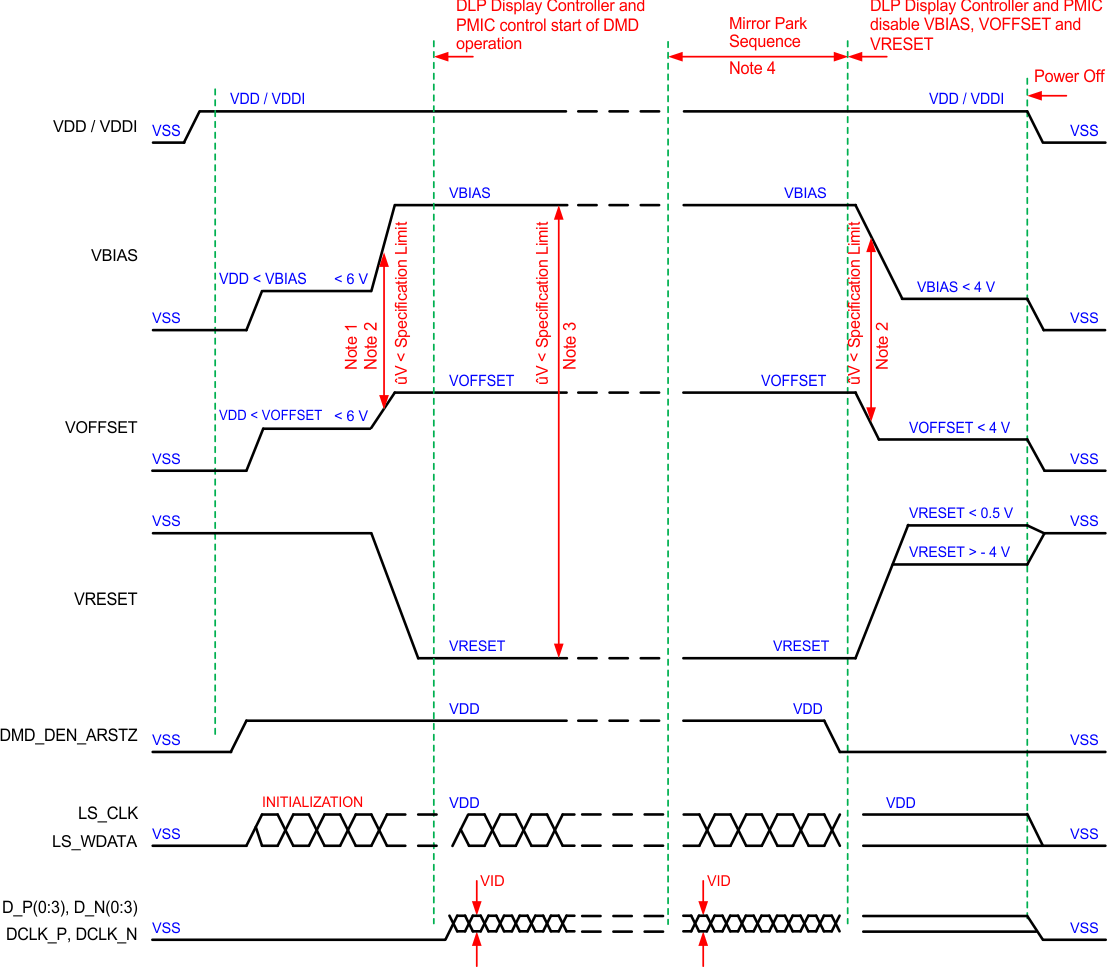
9.3 Power Supply Sequencing Requirements

B. To prevent excess current, the supply voltage
delta |VBIAS – VOFFSET| must be less than specified in
Section 6.4. OEMs may
find that the most reliable way to ensure this is to power VOFFSET
prior to VBIAS during power-up and to remove VBIAS prior
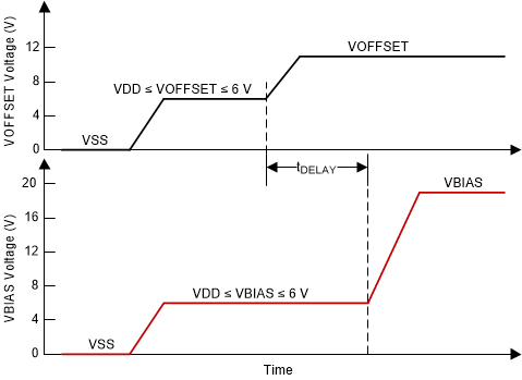
to VOFFSET during power-down. Refer to Table 9-1 and Figure 9-2 for power-up delay requirements.
C. To prevent excess current, the supply voltage
delta |VBIAS – VRESET| must be less than specified limit
shown in Section 6.4.
D. When system power is interrupted, the ASIC driver initiates hardware power-down that disables VBIAS, VRESET and VOFFSET after the Micromirror Park Sequence. Software power-down disables VBIAS, VRESET, and VOFFSET after the Micromirror Park Sequence through software control.
E. Drawing is not to scale and details are omitted for clarity.
Figure 9-1 Power Supply Sequencing Requirements (Power Up and Power Down)Table 9-1 Power-Up Sequence Delay Requirement
| PARAMETER | MIN | MAX | UNIT | |
|---|---|---|---|---|
| tDELAY | Delay requirement from VOFFSET power up to VBIAS power up | 2 | ms | |
| VOFFSET | Supply voltage level during power–up sequence delay (see Figure 9-2) | 6 | V | |
| VBIAS | Supply voltage level during power–up sequence delay (see Figure 9-2) | 6 | V | |

A. Refer to Table 9-1 for VOFFSET and VBIAS supply voltage levels during power-up sequence delay.
Figure 9-2 Power-Up Sequence Delay Requirement