ZHCSL02C March   2020  – March 2023 DLP3021-Q1

PRODUCTION DATA  

  1. 特性
  2. 应用
  3. 说明
  4. Revision History
  5. Pin Configuration and Functions
  6. Specifications
    1. 6.1  Absolute Maximum Ratings
    2. 6.2  Storage Conditions
    3. 6.3  ESD Ratings
    4. 6.4  Recommended Operating Conditions
    5. 6.5  Thermal Information
    6. 6.6  Electrical Characteristics
    7. 6.7  Timing Requirements
    8. 6.8  Switching Characteristics
    9. 6.9  System Mounting Interface Loads
    10. 6.10 Physical Characteristics of the Micromirror Array
    11. 6.11 Micromirror Array Optical Characteristics
    12. 6.12 Window Characteristics
    13. 6.13 Chipset Component Usage Specification
  7. Detailed Description
    1. 7.1 Overview
    2. 7.2 Functional Block Diagram
    3. 7.3 Feature Description
      1. 7.3.1 Micromirror Array
      2. 7.3.2 Double Data Rate (DDR) Interface
      3. 7.3.3 Micromirror Switching Control
      4. 7.3.4 DMD Voltage Supplies
      5. 7.3.5 Logic Reset
      6. 7.3.6 Temperature Sensing Diode
        1. 7.3.6.1 Temperature Sense Diode Theory
      7. 7.3.7 DMD JTAG Interface
    4. 7.4 System Optical Considerations
      1. 7.4.1 Numerical Aperture and Stray Light Control
      2. 7.4.2 Pupil Match
      3. 7.4.3 Illumination Overfill and Alignment
    5. 7.5 DMD Image Performance Specification
    6. 7.6 Micromirror Array Temperature Calculation
    7. 7.7 Micromirror Landed-On/Landed-Off Duty Cycle
  8. Application and Implementation
    1. 8.1 Application Information
    2. 8.2 Typical Application
    3. 8.3 Application Mission Profile Consideration
  9. Power Supply Recommendations
    1. 9.1 Power Supply Sequencing Requirements
      1. 9.1.1 Power Up and Power Down
  10. 10Layout
    1. 10.1 Layout Guidelines
    2. 10.2 Temperature Diode Pins
  11. 11Device and Documentation Support
    1. 11.1 Device Support
      1. 11.1.1 Device Nomenclature
      2. 11.1.2 Device Markings
    2. 11.2 Documentation Support
      1. 11.2.1 Related Documentation
    3. 11.3 接收文档更新通知
    4. 11.4 支持资源
    5. 11.5 Trademarks
    6. 11.6 静电放电警告
    7. 11.7 Device Handling
    8. 11.8 术语表
  12. 12Mechanical, Packaging, and Orderable Information

封装选项

机械数据 (封装 | 引脚)
散热焊盘机械数据 (封装 | 引脚)
订购信息

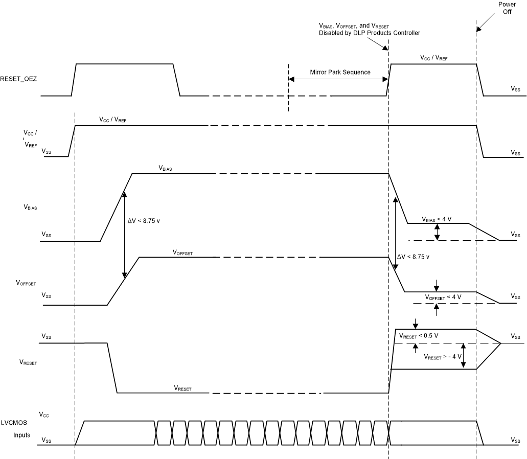
Power Up and Power Down

GUID-BA1593F1-2E94-48FC-BD94-274CAA27D5C4-low.gif
±8.75-V delta, ∆V, shall be considered the max operating delta between VBIAS and VOFFSET. Customers may find that the most reliable way to ensure this is to power VOFFSET prior to VBIAS during power up and to remove VBIAS prior to VOFFSET during power down.
Figure 9-1 Power Supply Sequencing Requirements (Power Up and Power Down)