ZHCSL02C March 2020 – March 2023 DLP3021-Q1
PRODUCTION DATA
- 1 特性
- 2 应用
- 3 说明
- 4 Revision History
- 5 Pin Configuration and Functions
-
6 Specifications
- 6.1 Absolute Maximum Ratings
- 6.2 Storage Conditions
- 6.3 ESD Ratings
- 6.4 Recommended Operating Conditions
- 6.5 Thermal Information
- 6.6 Electrical Characteristics
- 6.7 Timing Requirements
- 6.8 Switching Characteristics
- 6.9 System Mounting Interface Loads
- 6.10 Physical Characteristics of the Micromirror Array
- 6.11 Micromirror Array Optical Characteristics
- 6.12 Window Characteristics
- 6.13 Chipset Component Usage Specification
- 7 Detailed Description
- 8 Application and Implementation
- 9 Power Supply Recommendations
- 10Layout
- 11Device and Documentation Support
- 12Mechanical, Packaging, and Orderable Information
8.2 Typical Application
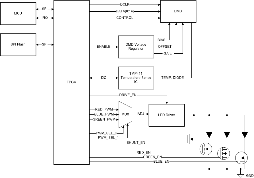
The DLP3021-Q1 DMD combined with a DLP products controller are the primary devices that make up the reference design for a dynamic ground projection system as shown in the block diagram Figure 8-1.
 Figure 8-1 Dynamic Ground Projection Reference Design Block Diagram
In this architecture, video content is compressed and stored in external flash memory. Low speed SPI commands are sent from a microcontroller or other processor to the DLP products controller to indicate what video content to read from external memory. Storing the video content in memory removes the need for a high speed video interface to the module which improves compatibility with typical vehicle infrastructures. It also decreases overall system size and cost by removing graphics generation and interfaces. The controller decompresses each bit plane of the video data (608 × 684 resolution) and displays them on the DMD in rapid succession to create the full video image. Due to the diamond format of the DMD pixels, the output image has an effective resolution of 864 × 480. The controller synchronizes the DMD bit plane data with the RGB enable timing for the LED color controller and driver circuit.
The controller may connect to a TMP411-Q1 to measure the DLP3021-Q1 temperature using the built-in temperature sensing diode.
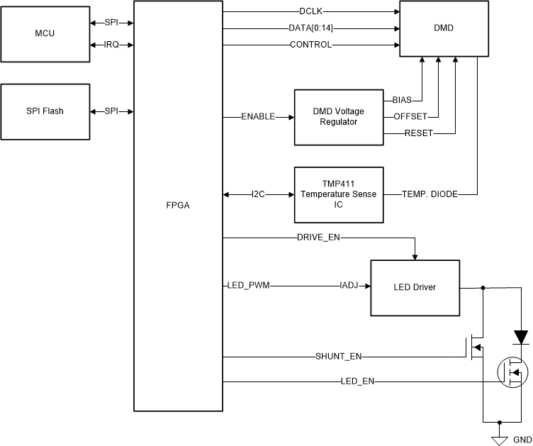
The controller combined with the DLP3021-Q1 may be used in RGB LED or laser illumination systems, or in single-color systems as shown in Figure 8-2.
 Figure 8-2 Dynamic Ground Projection Reference Design Block Diagram - Single Color