ZHCSL02C March 2020 – March 2023 DLP3021-Q1
PRODUCTION DATA
- 1 特性
- 2 应用
- 3 说明
- 4 Revision History
- 5 Pin Configuration and Functions
-
6 Specifications
- 6.1 Absolute Maximum Ratings
- 6.2 Storage Conditions
- 6.3 ESD Ratings
- 6.4 Recommended Operating Conditions
- 6.5 Thermal Information
- 6.6 Electrical Characteristics
- 6.7 Timing Requirements
- 6.8 Switching Characteristics
- 6.9 System Mounting Interface Loads
- 6.10 Physical Characteristics of the Micromirror Array
- 6.11 Micromirror Array Optical Characteristics
- 6.12 Window Characteristics
- 6.13 Chipset Component Usage Specification
- 7 Detailed Description
- 8 Application and Implementation
- 9 Power Supply Recommendations
- 10Layout
- 11Device and Documentation Support
- 12Mechanical, Packaging, and Orderable Information
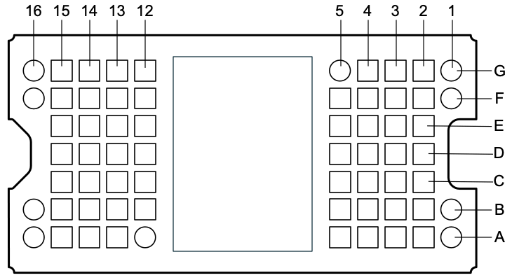
5 Pin Configuration and Functions
 Figure 5-1 FQR
Package,64-Pin LGA(Bottom View)
Figure 5-1 FQR
Package,64-Pin LGA(Bottom View)Table 5-1 Pin Functions
| PIN | TYPE | DESCRIPTION | |
|---|---|---|---|
| NAME | NO. | ||
| DATA(0) | A2 | LVCMOS input | Data bus. Synchronous to rising edge and falling edge of DCLK. |
| DATA(1) | A4 | ||
| DATA(2) | B2 | ||
| DATA(3) | B3 | ||
| DATA(4) | B5 | ||
| DATA(5) | C2 | ||
| DATA(6) | C3 | ||
| DATA(7) | B4 | ||
| DATA(8) | C5 | ||
| DATA(9) | D2 | ||
| DATA(10) | D3 | ||
| DATA(11) | D4 | ||
| DATA(12) | D5 | ||
| DATA(13) | E2 | ||
| DATA(14) | F5 | ||
| DCLK | F4 | Data clock. | |
| LOADB | F3 | Parallel latch load enable. Synchronous to rising edge and falling edge of DCLK. | |
| SCTRL | E4 | Serial control (sync). Synchronous to rising edge and falling edge of DCLK. | |
| TRC | F2 | Toggle rate control. Synchronous to rising edge and falling edge of DCLK. | |
| DAD_BUS | B15 | Reset control serial bus. Synchronous to rising edge of SAC_CLK. | |
| RESET_OEZ | C15 | Active low. Output enable signal for internal reset driver circuitry. | |
| RESET_STROBE | B13 | Rising edge on RESET_STROBE latches in the control signals. | |
| SAC_BUS | A15 | Stepped address control serial bus. Synchronous to rising edge of SAC_CLK. | |
| SAC_CLK | A14 | Stepped address control clock. | |
| TCK | F15 | JTAG clock. | |
| TDI | E13 | JTAG data input. Synchronous to rising edge of TCK. Bond pad connects to internal pull up resistor. | |
| TDO | G15 | LVCMOS output | JTAG data output. Synchronous to falling edge of TCK. Tri-state failsafe output buffer. |
| TMS | G14 | LVCMOS input | JTAG mode select. Synchronous to rising edge of TCK. Bond pad connects to internal pull up resistor. |
| TEMP_MINUS | G13 | Analog input | Calibrated temperature diode used to assist accurate temperature measurements of DMD die. |
| TEMP_PLUS | G2 | ||
| VBIAS | D15 | Power | Power supply for positive bias level of mirror reset signal. |
| VCC | A5, B12, C14, D12, F13, G3 | Power supply for low voltage CMOS logic. Power supply for normal high voltage at mirror address electrodes. Power supply for offset level of mirror reset signal during power down. | |
| VOFFSET | E14 | Power | Power supply for high voltage CMOS logic. Power supply for stepped high voltage at mirror address electrodes. Power supply for offset level of mirror reset signal. |
| VREF | E15 | Power supply for low voltage CMOS DDR interface. | |
| VRESET | D14 | Power supply for negative reset level of mirror reset signal. | |
| VSS | A3, A13, B14, C4, C12, C13, D13, E3, E5, E12, F12, F14, G4, G12 | Common return for all power. | |
| RESERVED | A1, A12, A16,B1, B16, F1, F16, G1, G5, G16 | Reserved | Do not connect. |