ZHCSJL8A April 2019 – September 2019 DLP3034-Q1
PRODUCTION DATA.
- 1 特性
- 2 应用
- 3 说明
- 4 修订历史记录
- 5 Pin Configuration and Functions
-
6 Specifications
- 6.1 Absolute Maximum Ratings
- 6.2 Storage Conditions
- 6.3 ESD Ratings
- 6.4 Recommended Operating Conditions
- 6.5 Thermal Information
- 6.6 Electrical Characteristics
- 6.7 Timing Requirements
- 6.8 Switching Characteristics
- 6.9 System Mounting Interface Loads
- 6.10 Physical Characteristics of the Micromirror Array
- 6.11 Micromirror Array Optical Characteristics
- 6.12 Window Characteristics
- 6.13 Chipset Component Usage Specification
- 7 Detailed Description
- 8 Application and Implementation
- 9 Power Supply Recommendations
- 10Layout
- 11器件和文档支持
- 12机械、封装和可订购信息
6.4 Recommended Operating Conditions
Over operating free-air temperature range (unless otherwise noted)| MIN | NOM | MAX | UNIT | ||||
|---|---|---|---|---|---|---|---|
| SUPPLY VOLTAGE RANGE | |||||||
| VREF | LVCMOS interface power supply voltage(3) | 1.65 | 1.8 | 1.95 | V | ||
| VCC | LVCMOS logic power supply voltage(3) | 2.25 | 2.5 | 2.75 | V | ||
| VOFFSET | Mirror electrode and HVCMOS voltage(3) | 8.25 | 8.5 | 8.75 | V | ||
| VBIAS | Mirror electrode voltage | 15.5 | 16 | 16.5 | V | ||
| |VBIAS – VOFFSET| | Supply voltage delta(2) | 8.75 | V | ||||
| VRESET | Mirror electrode voltage | –9.5 | –10 | –10.5 | V | ||
| VP VT+ | Positive going threshold voltage | 0.4 × VREF | 0.7 × VREF | V | |||
| VN VT– | Negative going threshold voltage | 0.3 × VREF | 0.6 × VREF | V | |||
| VH ∆VT | Hysteresis voltage (Vp – Vn) | 0.1 × VREF | 0.4 × VREF | V | |||
| IOH_TDO | High level output current @ Voh = 2.25 V, TDO, Vcc = 2.25 V | –2 | mA | ||||
| IOL_TDO | Low level output current @ Vol = 0.4 V, TDO, Vcc = 2.25 V | 2 | mA | ||||
| TEMPERATURE DIODE | |||||||
| ITEMP_DIODE | Max current source into temperature diode(4) | 120 | µA | ||||
| ENVIRONMENTAL | |||||||
| TARRAY | Operating DMD array temperature (1) | –40 | 105 | °C | |||
| ILLsub-385nm | Illumination, wavelength < 385 nm | 2.0 | mW/cm2 | ||||
| ILL385-to-395nm | Illumination, 385 nm < wavelength < 395 nm | 250 | mW/cm2 | ||||
| ILL395-to-400nm | Illumination, 395 nm < wavelength < 400 nm | 800 | mW/cm2 | ||||
| ILL400-to-420nmnm | Illumination, 400 nm < wavelength < 420 nm | 8.0 | W/cm2 | ||||
| ILLVIS | Illumination, 420 nm < wavelength < 800 nm | Thermally limited(5) | W/cm2 | ||||
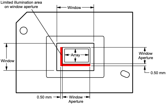
| ILLOVERFILL | Illumination overfill maximum heat load in areas shown in Figure 1(6) | TARRAY ≤ 75°C | 26 | mW/mm2 | |||
| Illumination overfill maximum heat load in areas shown in Figure 1(6) | TARRAY > 75°C | 20 | mW/mm2 | ||||
(1) DMD active array temperature can be calculated as shown in Micromirror Array Temperature Calculation section. Additionally, the DMD array temperature is monitored in the system using the TMP411-Q1 and DLPC120-Q1 as shown in the system block diagram.
(2) To prevent excess current, the supply voltage delta |VBIAS – VOFFSET| must be less than or equal to 8.75 V.
(3) VBIAS, VCC, VOFFSET, VREF, VRESET, VSS are required to operate the DMD.
(4) Temperature Diode is to allow accurate measurement of the DMD array temperature during operation.
(5) Limited by the resulting micromirror array temperature. Refer to the calculation example in Micromirror Array Temperature Calculation section.
(6) The active area of the DLP303x-Q1 device is surrounded by an aperture on the inside of the DMD window surface that masks structures of the DMD device assembly from normal view. The aperture is sized to anticipate several optical conditions. Overfill light illuminating the area outside the active array can scatter and create adverse effects to the performance of an end application using the DMD. The illumination optical system should be designed to minimize light flux incident outside the active array. Depending on the particular system's optical architecture and assembly tolerances, the amount of overfill light on the outside of the active array may cause system performance degradation.
 Figure 1. Illumination Overfill Diagram