ZHCSJL8A April 2019 – September 2019 DLP3034-Q1
PRODUCTION DATA.
- 1 特性
- 2 应用
- 3 说明
- 4 修订历史记录
- 5 Pin Configuration and Functions
-
6 Specifications
- 6.1 Absolute Maximum Ratings
- 6.2 Storage Conditions
- 6.3 ESD Ratings
- 6.4 Recommended Operating Conditions
- 6.5 Thermal Information
- 6.6 Electrical Characteristics
- 6.7 Timing Requirements
- 6.8 Switching Characteristics
- 6.9 System Mounting Interface Loads
- 6.10 Physical Characteristics of the Micromirror Array
- 6.11 Micromirror Array Optical Characteristics
- 6.12 Window Characteristics
- 6.13 Chipset Component Usage Specification
- 7 Detailed Description
- 8 Application and Implementation
- 9 Power Supply Recommendations
- 10Layout
- 11器件和文档支持
- 12机械、封装和可订购信息
7.3.7 DMD JTAG Interface
The DMD uses 4 standard JTAG signals for sending and receiving boundary scan test data. TCK is the test clock used to drive an IEEE 1149.1 TAP state machine and logic. TMS directs the next state of the TAP state machine. TDI is the scan data input and TDO is the scan data output.
The DMD does not support IEEE 1149.1 signals TRST (Test Logic Reset) and RTCK (Returned Test Clock). Boundary scan cells on the DMD are Observe-Only. To initiate the JTAG boundary scan operation on the DMD, a minimum of 6 TCK clock cycles are required after TMS is set to logic high.
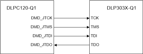
Refer to Figure 13 for a JTAG system board routing example. The DLPC120-Q1 can be enabled to perform an in system boundary scan test. See DLPC120-Q1 Programmer's Guide for information about this test.
 Figure 13. System Interface Connection to DLPC120-Q1
 The DMD Device ID can be read via the JTAG interface. The ID and 32-bit shift order is shown in Figure 14.
 Figure 14. DMD Device ID and 32-bit Shift Order
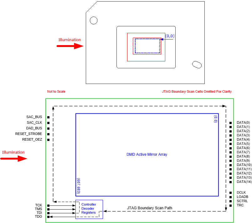
 Refer to Figure 15 for a JTAG boundary scan block diagram for the DMD. These show the pins and the scan order that are observed during the JTAG boundary scan.
 Figure 15. JTAG Boundary Scan Path
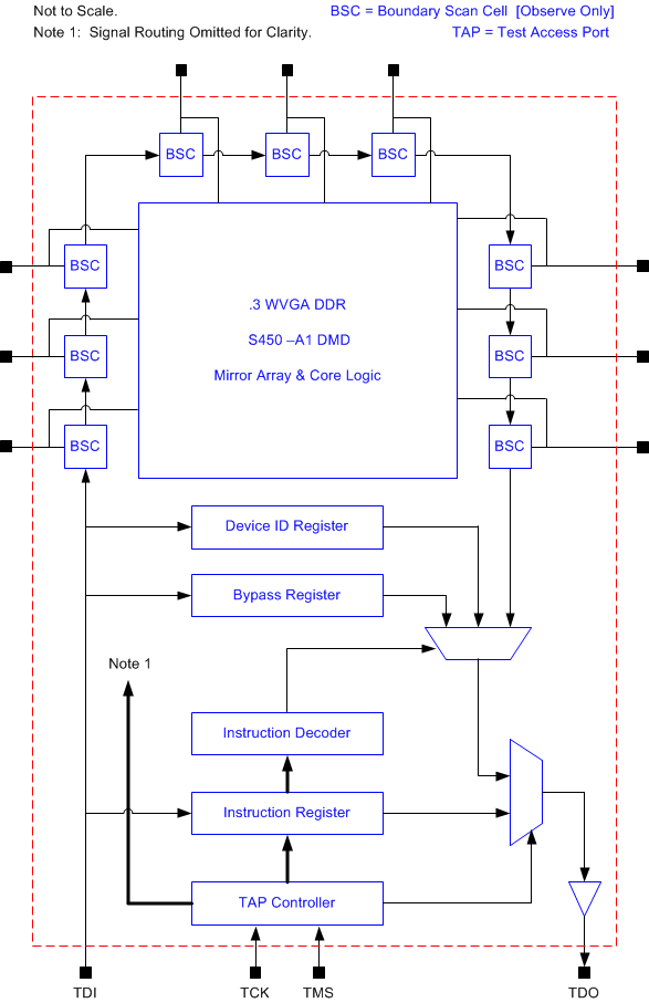
 Refer to Figure 16 for a functional block diagram of the JTAG control logic.
 Figure 16. JTAG Functional Block Diagram