ZHCSJL8A April 2019 – September 2019 DLP3034-Q1
PRODUCTION DATA.
- 1 特性
- 2 应用
- 3 说明
- 4 修订历史记录
- 5 Pin Configuration and Functions
-
6 Specifications
- 6.1 Absolute Maximum Ratings
- 6.2 Storage Conditions
- 6.3 ESD Ratings
- 6.4 Recommended Operating Conditions
- 6.5 Thermal Information
- 6.6 Electrical Characteristics
- 6.7 Timing Requirements
- 6.8 Switching Characteristics
- 6.9 System Mounting Interface Loads
- 6.10 Physical Characteristics of the Micromirror Array
- 6.11 Micromirror Array Optical Characteristics
- 6.12 Window Characteristics
- 6.13 Chipset Component Usage Specification
- 7 Detailed Description
- 8 Application and Implementation
- 9 Power Supply Recommendations
- 10Layout
- 11器件和文档支持
- 12机械、封装和可订购信息
8.2 Typical Application
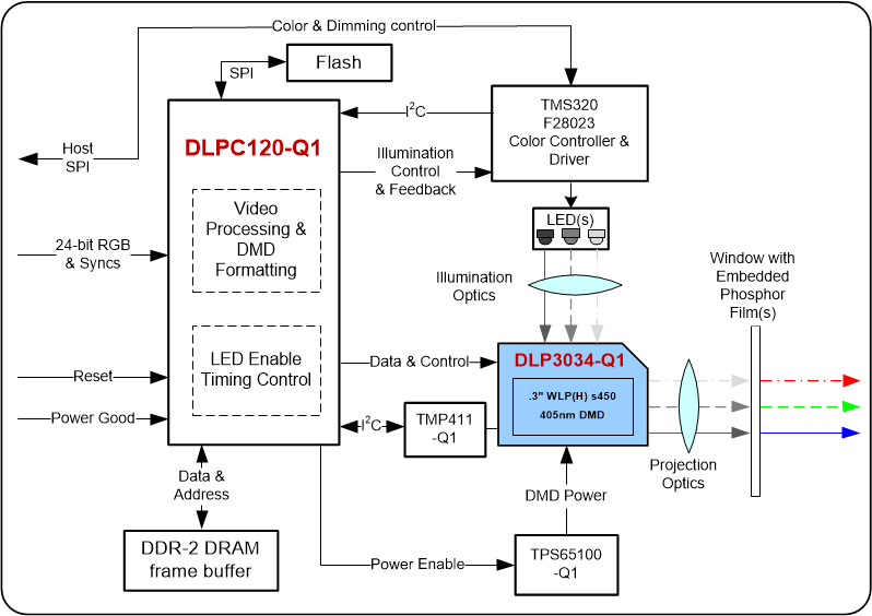
The DLP3034-Q1 DMD combined with the DLPC120-Q1 are the primary devices that make up the reference design for a transparent window display system as shown in the block diagram Figure 18.
 Figure 18. DLP3034-Q1 Reference Design Block Diagram
 The DLPC120-Q1 accepts input video over the parallel RGB data interface up to 8 bits per color from a Video Graphics processor. The DLPC120-Q1 then processes the video data (864 × 480 manhattan orientation) by scaling the image to match the DMD resolution (608 × 684 diamond pixel), applies de-gamma correction, bezel adjustment, and then formats the data into DMD bit plane information and stores the data into the DDR2 DRAM. The DMD bit planes are read from DDR2 DRAM, and are then displayed on the DMD using Pulse Width Modulation (PWM) timing. The DLPC120-Q1 synchronizes the DMD bit plane data with the color enable timing for the LED color controller and Driver circuit. Finally, the DMD accepts the bit plane formatted data from the DLPC120-Q1 and displays the data according to the timing controlled by the DLPC120-Q1.
Due to the mechanical nature of the micromirrors, the latency of the DLP3034-Q1 and DLPC120-Q1 chipset is fixed across all temperature and operating conditions. The observed video latency is one frame, or 16.67 ms at an input frame rate of 60 Hz. However, please note that the use of the DLPC120-Q1 bezel adjustment feature, if enabled by the host controller, requires an additional frame of processing.
The DLPC120-Q1 is configured at power up by data stored in the flash file which stores configuration data, DMD and sequence timing information, LED drive information, and other information related to the system functions. See the DLPC120-Q1 Programmer's Guide for information about the this flash configuration data.
The transparent emissive display reference design from TI includes the TMS320F28023 Microcontroller (Piccolo), which is used to adjust the LED current levels in order to control the brightness levels and also the color point for systems with multiple color channels.