ZHCSJA4B January 2019 – May 2022 DLP4500
PRODUCTION DATA
- 1 特性
- 2 应用
- 3 说明
- 4 Revision History
- 5 Chipset Component Usage Specification
- 6 Pin Configuration and Functions
-
7 Specifications
- 7.1 Absolute Maximum Ratings
- 7.2 Storage Conditions
- 7.3 ESD Ratings
- 7.4 Recommended Operating Conditions
- 7.5 Thermal Information
- 7.6 Electrical Characteristics
- 7.7 Timing Requirements
- 7.8 System Mounting Interface Loads
- 7.9 Micromirror Array Physical Characteristics
- 7.10 Micromirror Array Optical Characteristics
- 7.11 Typical Characteristics
- 8 Detailed Description
- 9 Application and Implementation
- 10Power Supply Recommendations
-
11Layout
- 11.1 Layout Guidelines
- 11.2 Layout Example
- 12Device and Documentation Support
- 13Mechanical, Packaging, and Orderable Information
11.2.3 Recommended DLPC350 PLL Layout Configuration
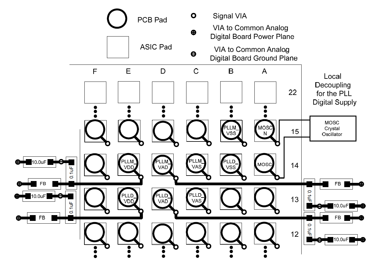
High-frequency decoupling is required for both 1.2-V and 1.8-V PLL supplies and should be provided as close as possible to each of the PLL supply package pins as shown in the example layout in Figure 11-4. TI recommends that decoupling capacitors be placed under the package on the opposite side of the board. High quality, low-ESR, monolithic, surface mount capacitors should be used. Typically 0.1 µF for each PLL supply should be sufficient. The length of a connecting trace increases the parasitic inductance of the mounting and thus, where possible, there should be no trace, allowing the via to butt up against the land itself. Additionally, the connecting trace should be made as wide as possible. Further improvement can be made by placing vias to the side of the capacitor lands or doubling the number of vias.
The location of bulk decoupling depends on the system design. Typically, a good ceramic capacitor in the 10-µF range is adequate.
 Figure 11-4 PLL Filter Layout