ZHCSJA3B January 2019 – May 2022 DLP4500NIR
PRODUCTION DATA
- 1 特性
- 2 应用范围
- 3 说明
- 4 Revision History
- 5 Chipset Component Usage Specification
- 6 Pin Configuration and Functions
-
7 Specifications
- 7.1 Absolute Maximum Ratings
- 7.2 Storage Conditions
- 7.3 ESD Ratings
- 7.4 Recommended Operating Conditions
- 7.5 Thermal Information
- 7.6 Electrical Characteristics
- 7.7 Timing Requirements
- 7.8 System Mounting Interface Loads
- 7.9 Micromirror Array Physical Characteristics
- 7.10 Micromirror Array Optical Characteristics
- 7.11 Typical Characteristics
- 8 Detailed Description
- 9 Applications and Implementation
- 10Power Supply Recommendations
-
11Layout
- 11.1 Layout Guidelines
- 11.2 Layout Example
- 12Device and Documentation Support
- 13Mechanical, Packaging, and Orderable Information
8.3 Feature Description
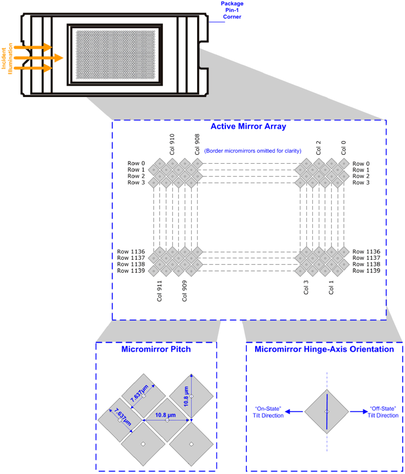
Each aluminum micromirror is approximately 7.6 microns in size and arranged in row and columns as shown in Figure 8-1. Due to the diamond pixel array of the DMD, the pixel data does not appear on the DMD exactly as it would in an orthogonal pixel arrangement. Pixel arrangement and numbering for the DLP4500NIR is shown in Figure 8-1.
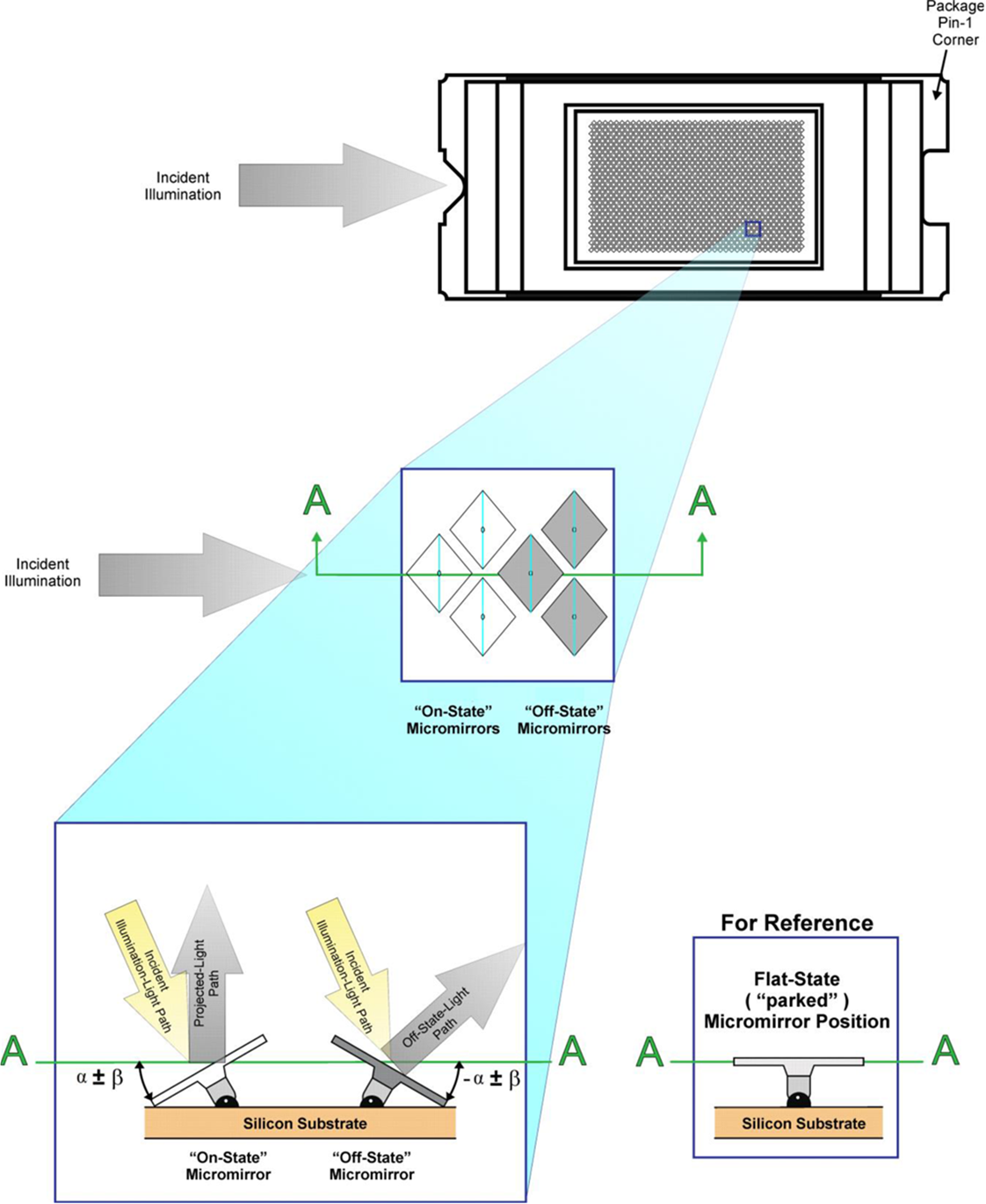
Each micromirror is switchable between two discrete angular positions: –12° and 12°. The angular positions α and β are measured relative to a 0° flat reference when the mirrors are parked in their inactive state, parallel to the array plane (see Figure 8-2). The parked position is not a latched position. Individual micromirror angular positions are relatively flat, but do vary. The tilt direction is perpendicular to the hinge-axis. The on-state landed position is directed toward the left side of the package (see Figure 8-2).
 Figure 8-1 Micromirror Array, Pitch, and
Hinge-Axis Orientation
 Figure 8-2 Micromirror Landed Positions
and Light Paths
Figure 8-2 Micromirror Landed Positions
and Light PathsEach individual micromirror is positioned over a corresponding CMOS memory cell. The angular position of a specific micromirror is determined by the binary state (logic 0 or 1) of the corresponding CMOS memory cell contents, after the mirror clocking pulse is applied. The angular position (–12° or 12°) of the individual micromirrors changes synchronously with a micromirror clocking pulse, rather than being coincident with the CMOS memory cell data update. Therefore, writing a logic 1 into a memory cell followed by a mirror clocking pulse results in the corresponding micromirror switching to a 12° position. Writing a logic 0 into a memory cell followed by a mirror clocking pulse results in the corresponding micromirror switching to a –12° position.
Updating the angular position of the micromirror array consists of two steps.
- Update the contents of the CMOS memory.
- Applying a mirror clocking pulse to the entire micromirror array.
Mirror reset pulses are generated internally by the DLP4500NIR DMD, with initiation of the pulses being coordinated by the DLPC350 controller. For timing specifications, see Section 7.7.
Around the perimeter of the 912 × 1140 array of micromirrors is a uniform band of border micromirrors. The border micromirrors are not user-addressable. The border micromirrors land in the –12° position after power has been applied to the device. There are 10 border micromirrors on each side of the 912 × 1140 active array.