ZHCSJA3B January   2019  – May 2022 DLP4500NIR

PRODUCTION DATA  

  1. 特性
  2. 应用范围
  3. 说明
  4. Revision History
  5. Chipset Component Usage Specification
  6. Pin Configuration and Functions
  7. Specifications
    1. 7.1  Absolute Maximum Ratings
    2. 7.2  Storage Conditions
    3. 7.3  ESD Ratings
    4. 7.4  Recommended Operating Conditions
    5. 7.5  Thermal Information
    6. 7.6  Electrical Characteristics
    7. 7.7  Timing Requirements
    8. 7.8  System Mounting Interface Loads
    9. 7.9  Micromirror Array Physical Characteristics
    10. 7.10 Micromirror Array Optical Characteristics
    11. 7.11 Typical Characteristics
  8. Detailed Description
    1. 8.1 Overview
    2. 8.2 Functional Block Diagram
    3. 8.3 Feature Description
    4. 8.4 Device Functional Modes
      1. 8.4.1 Operating Modes
    5. 8.5 Micromirror Array Temperature Calculation
      1. 8.5.1 Package Thermal Resistance
      2. 8.5.2 Case Temperature
        1. 8.5.2.1 Temperature Calculation
    6. 8.6 Micromirror Landed-on/Landed-Off Duty Cycle
      1. 8.6.1 Definition of Micromirror Landed-On/Landed-Off Duty Cycle
      2. 8.6.2 Landed Duty Cycle and Useful Life of the DMD
      3. 8.6.3 Landed Duty Cycle and Operational DMD Temperature
      4. 8.6.4 Estimating the Long-Term Average Landed Duty Cycle of a Product or Application
  9. Applications and Implementation
    1. 9.1 Application Information
    2. 9.2 Typical Application
      1. 9.2.1 Design Requirements
      2. 9.2.2 Detailed Design Procedure
        1. 9.2.2.1 DLPC350 System Interfaces
          1. 9.2.2.1.1 Control Interface
          2. 9.2.2.1.2 Input Data Interface
        2. 9.2.2.2 DLPC350 System Output Interfaces
          1. 9.2.2.2.1 Illumination Interface
          2. 9.2.2.2.2 Trigger Interface (Sync Outputs)
        3. 9.2.2.3 DLPC350 System Support Interfaces
          1. 9.2.2.3.1 Reference Clock
          2. 9.2.2.3.2 PLL
          3. 9.2.2.3.3 Program Memory Flash Interface
        4. 9.2.2.4 DMD Interfaces
          1. 9.2.2.4.1 DLPC350 to DMD Digital Data
          2. 9.2.2.4.2 DLPC350 to DMD Control Interface
          3. 9.2.2.4.3 DLPC350 to DMD Micromirror Reset Control Interface
  10. 10Power Supply Recommendations
    1. 10.1 Power Supply Sequencing Requirements
    2. 10.2 DMD Power Supply Power-Up Procedure
    3. 10.3 DMD Power Supply Power-Down Procedure
  11. 11Layout
    1. 11.1 Layout Guidelines
      1. 11.1.1 DMD Interface Design Considerations
      2. 11.1.2 DMD Termination Requirements
      3. 11.1.3 Decoupling Capacitors
      4. 11.1.4 Power Plane Recommendations
      5. 11.1.5 Signal Layer Recommendations
      6. 11.1.6 General Handling Guidelines for CMOS-Type Pins
      7. 11.1.7 PCB Manufacturing
        1. 11.1.7.1 General Guidelines
        2. 11.1.7.2 Trace Widths and Minimum Spacings
        3. 11.1.7.3 Routing Constraints
        4. 11.1.7.4 Fiducials
        5. 11.1.7.5 Flex Considerations
        6. 11.1.7.6 DLPC350 Thermal Considerations
    2. 11.2 Layout Example
      1. 11.2.1 Printed Circuit Board Layer Stackup Geometry
      2. 11.2.2 Recommended DLPC350 MOSC Crystal Oscillator Configuration
      3. 11.2.3 Recommended DLPC350 PLL Layout Configuration
  12. 12Device and Documentation Support
    1. 12.1 Device Support
      1. 12.1.1 第三方米6体育平台手机版_好二三四免责声明
      2. 12.1.2 Device Nomenclature
      3. 12.1.3 Device Markings
    2. 12.2 Documentation Support
      1. 12.2.1 Related Documentation
    3. 12.3 接收文档更新通知
    4. 12.4 支持资源
    5. 12.5 Trademarks
    6. 12.6 Electrostatic Discharge Caution
    7. 12.7 术语表
  13. 13Mechanical, Packaging, and Orderable Information

封装选项

机械数据 (封装 | 引脚)
散热焊盘机械数据 (封装 | 引脚)
订购信息

Micromirror Array Physical Characteristics

VALUE UNIT
Number of active micromirror rows (2)1140micromirrors
Number of active micromirror columns (2)912micromirrors
Micromirror pitch, diagonal (2)7.6µm
Micromirror pitch, vertical and horizontal (2)10.8µm
Micromirror active array height (3)1140micromirrors
6161.4µm
Micromirror active array width (3)912micromirrors
9855µm
Micromirror array border (1)10mirrors/side
The mirrors that form the array border are hard-wired to tilt in the –12° (“Off”) direction once power is applied to the DMD (see Micromirror Array, Pitch, and Hinge-Axis Orientation and Micromirror Landed Positions and Light Paths).
See Micromirror Active Area in Figure 7-4.
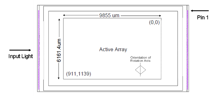
GUID-0E62BD98-08DB-485D-A9FD-FB744F382B6D-low.pngFigure 7-4 DLP4500NIR Micromirror Active Area