ZHCSJ13B November 2018 – May 2022 DLP4710
PRODUCTION DATA
- 1 特性
- 2 应用
- 3 说明
- 4 Revision History
- 5 Pin Configuration and Functions
-
6 Specifications
- 6.1 Absolute Maximum Ratings
- 6.2 Storage Conditions
- 6.3 ESD Ratings
- 6.4 Recommended Operating Conditions
- 6.5 Thermal Information
- 6.6 Electrical Characteristics
- 6.7 Timing Requirements
- 6.8 Switching Characteristics
- 6.9 System Mounting Interface Loads
- 6.10 Physical Characteristics of the Micromirror Array
- 6.11 Micromirror Array Optical Characteristics
- 6.12 Window Characteristics
- 6.13 Chipset Component Usage Specification
- 6.14 Software Requirements
- 7 Detailed Description
- 8 Application and Implementation
- 9 Power Supply Recommendations
- 10Layout
- 11Device and Documentation Support
- 12Mechanical, Packaging, and Orderable Information
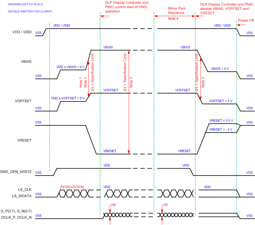
9.3 Power Supply Sequencing Requirements

A. DLP controller and PMIC controls
start of DMD operation
B. Mirror park sequence starts
C. Mirror park sequence ends. DLP
controller and PMIC disables VBIAS, VOFFSET, and VRESET.
D. Power off.
F. When system power is interrupted,
the ASIC driver initiates hardware the power-down sequence, that disables VBIAS,
VRESET and VOFFSET after the micromirror park sequence is complete. Software the
power-down sequence, disables VBIAS, VRESET, and VOFFSET after the micromirror
park sequence through software control.
G. To prevent excess current, the
supply voltage delta |VBIAS – VRESET| must be less than specified limit shown in
Section 6.4.
H. Drawing is not to scale and
details are omitted for clarity.
Figure 9-1 Power Supply Sequencing
Requirements (Power Up and Power Down)Table 9-1 Power-Up Sequence Delay
Requirement
| PARAMETER | MIN | MAX | UNIT | |
|---|---|---|---|---|
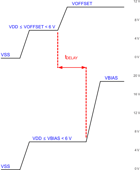
| tDELAY | Delay requirement from VOFFSET power up to VBIAS power up | 2 | ms | |
| VOFFSET | Supply voltage level during power–up sequence delay (see Figure 9-2) | 6 | V | |
| VBIAS | Supply voltage level during power–up sequence delay (see Figure 9-2) | 6 | V | |

A. Refer to Table 9-1 for VOFFSET and VBIAS supply voltage levels during power-up sequence
delay.
Figure 9-2 Power-Up Sequence Delay
Requirement