ZHCSIG0G April 2016 – May 2019 DLP5531-Q1
PRODUCTION DATA.
- 1 特性
- 2 应用
- 3 说明
- 4 修订历史记录
- 5 Pin Configuration and Functions
-
6 Specifications
- 6.1 Absolute Maximum Ratings
- 6.2 Storage Conditions
- 6.3 ESD Ratings
- 6.4 Recommended Operating Conditions
- 6.5 Thermal Information
- 6.6 Electrical Characteristics
- 6.7 Timing Requirements
- 6.8 Switching Characteristics
- 6.9 System Mounting Interface Loads
- 6.10 Physical Characteristics of the Micromirror Array
- 6.11 Micromirror Array Optical Characteristics
- 6.12 Window Characteristics
- 6.13 Chipset Component Usage Specification
- 7 Detailed Description
- 8 Application and Implementation
- 9 Power Supply Recommendations
- 10Layout
- 11器件和文档支持
- 12机械、封装和可订购信息
7.1 Overview
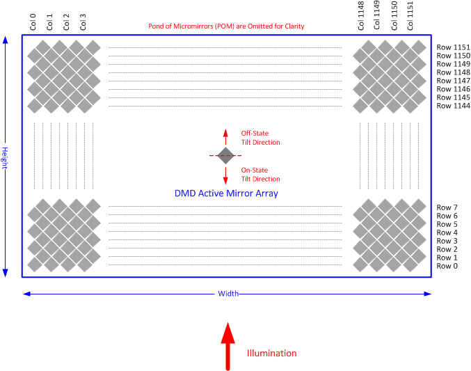
The DLP5531-Q1 Automotive DMD consists of 1,327,104 highly reflective, digitally switchable, micrometer-sized mirrors organized in a two-dimensional array. As shown in Figure 15, the micromirror array consists of 1152 micromirror columns × 1152 micromirror rows in a diamond pixel configuration with a 2:1 aspect ratio.
Around the perimeter of the 1152 × 1152 array of micromirrors is a uniform band of border micromirrors called the Pond of Micromirrors (POM). The border micromirrors are not user-addressable. The border micromirrors land in the –12° position once power has been applied to the device. There are 10 border micromirrors on each side of the 1152 × 1152 active array.
Due to the diamond pixel configuration, the columns of each odd row are offset by half a pixel from the columns of the even row. Each mirror is switchable between two discrete angular positions: –12° and +12°. The mirrors are illuminated from the bottom which allows for compact and efficient system optical design.
Although the native resolution of the DLP5531-Q1 is 1152 × 1152, when paired with the DLPC230-Q1 controller, the DLP5531-Q1 can be driven with different resolutions to utilize the 2:1 aspect ratio. For example, Headlight applications typically use a resolution of 1152 × 576. Please see the DLPC230-Q1 automotive DMD controller data sheet (DLPS054) for a list of supported resolutions.
 Figure 15. 0.55-in 1.3-MP Micromirror Array