ZHCSNP3A September   2020  – April 2021 DLP5533A-Q1

PRODUCTION DATA  

  1. 特性
  2. 应用
  3. 说明
  4. Revision History
  5. Pin Configuration and Functions
  6. Specifications
    1. 6.1  Absolute Maximum Ratings
    2. 6.2  Storage Conditions
    3. 6.3  ESD Ratings
    4. 6.4  Recommended Operating Conditions
    5.     Illumination Overfill Diagram
    6. 6.5  Thermal Information
    7. 6.6  Electrical Characteristics
    8. 6.7  Timing Requirements
    9.     Electrical and Timing Diagrams
    10. 6.8  Switching Characteristics
    11.     LPSDR and Test Load Circuit Diagrams
    12. 6.9  System Mounting Interface Loads
    13.     System Interface Loads Diagram
    14. 6.10 Physical Characteristics of the Micromirror Array
    15.     Array Physical Characteristics Diagram
    16. 6.11 Micromirror Array Optical Characteristics
    17. 6.12 Window Characteristics
    18. 6.13 Chipset Component Usage Specification
  7. Detailed Description
    1. 7.1 Overview
    2. 7.2 Functional Block Diagram
    3. 7.3 Feature Description
      1. 7.3.1 Sub-LVDS Data Interface
      2. 7.3.2 Low Speed Interface for Control
      3. 7.3.3 DMD Voltage Supplies
      4. 7.3.4 Asynchronous Reset
      5. 7.3.5 Temperature Sensing Diode
        1. 7.3.5.1 Temperature Sense Diode Theory
    4. 7.4 System Optical Considerations
      1. 7.4.1 Numerical Aperture and Stray Light Control
      2. 7.4.2 Pupil Match
      3. 7.4.3 Illumination Overfill
    5. 7.5 DMD Image Performance Specification
    6. 7.6 Micromirror Array Temperature Calculation
      1. 7.6.1 Temperature Rise Through the Package for Heatsink Design
      2. 7.6.2 Monitoring Array Temperature Using the Temperature Sense Diode
    7. 7.7 Micromirror Landed-On/Landed-Off Duty Cycle
      1. 7.7.1 Definition of Micromirror Landed-On/Landed-Off Duty Cycle
  8. Application and Implementation
    1. 8.1 Application Information
    2. 8.2 Typical Application
      1. 8.2.1 Application Overview
      2. 8.2.2 Reference Design
      3. 8.2.3 Application Mission Profile Consideration
  9. Power Supply Recommendations
    1. 9.1 Power Supply Power-Up Procedure
    2. 9.2 Power Supply Power-Down Procedure
    3. 9.3 Power Supply Sequencing Requirements
  10. 10Layout
    1. 10.1 Layout Guidelines
  11. 11Device and Documentation Support
    1. 11.1 Device Support
      1. 11.1.1 Device Nomenclature
      2. 11.1.2 Device Markings
    2. 11.2 接收文档更新通知
    3. 11.3 支持资源
    4. 11.4 Trademarks
    5. 11.5 静电放电警告
    6. 11.6 DMD Handling
    7. 11.7 术语表
  12. 12Mechanical, Packaging, and Orderable Information

封装选项

机械数据 (封装 | 引脚)
散热焊盘机械数据 (封装 | 引脚)
订购信息

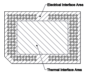
System Interface Loads Diagram

GUID-0CF05E07-E3B0-4269-B283-04127004438F-low.gif Figure 6-12 System Interface Loads