ZHCSK93 September 2019 DLP5534-Q1
ADVANCE INFORMATION for pre-production products; subject to change without notice.
- 1 特性
- 2 应用
- 3 说明
- 4 修订历史记录
- 5 Pin Configuration and Functions
-
6 Specifications
- 6.1 Absolute Maximum Ratings
- 6.2 Storage Conditions
- 6.3 ESD Ratings
- 6.4 Recommended Operating Conditions
- 6.5 Thermal Information
- 6.6 Electrical Characteristics
- 6.7 Timing Requirements
- 6.8 Switching Characteristics
- 6.9 System Mounting Interface Loads
- 6.10 Physical Characteristics of the Micromirror Array
- 6.11 Micromirror Array Optical Characteristics
- 6.12 Window Characteristics
- 6.13 Chipset Component Usage Specification
- 7 Detailed Description
- 8 Application and Implementation
- 9 Power Supply Recommendations
- 10Layout
- 11器件和文档支持
- 12机械、封装和可订购信息
6.7 Timing Requirements
Device electrical characteristics are over Recommended Operating Conditions unless otherwise noted| MIN | NOM | MAX | UNIT | |||
|---|---|---|---|---|---|---|
| LPSDR | ||||||
| tr | Rise slew rate(1) | (20% to 80%) × VDD, see Figure 2 | 0.25 | V/ns | ||
| tƒ | Fall slew rate(1) | (80% to 20%) × VDD, see Figure 2 | 0.25 | V/ns | ||
| tW(H) | Pulse duration LS_CLK high | 50% to 50% reference points, see Figure 4 | 0.75 | ns | ||
| tW(L) | Pulse duration LS_CLK low | 50% to 50% reference points, see Figure 4 | 0.75 | ns | ||
| tsu | Setup time | LS_WDATA valid before LS_CLK ↑ or LS_CLK ↓,
see Figure 4 |
1.5 | ns | ||
| th | Hold time | LS_WDATA valid after LS_CLK ↑ or LS_CLK ↓,
see Figure 4 |
1.5 | ns | ||
| SubLVDS | ||||||
| tr | Rise slew rate | 20% to 80% reference points, see Figure 3 | 0.7 | 1 | V/ns | |
| tƒ | Fall slew rate | 80% to 20% reference points, see Figure 3 | 0.7 | 1 | V/ns | |
| tc | Cycle time DCLK | See Figure 4 | 1.61 | 1.67 | ns | |
| tW(H) | Pulse duration DCLK high | 50% to 50% reference points, see Figure 4 | 0.75 | ns | ||
| tW(L) | Pulse duration DCLK low | 50% to 50% reference points, see Figure 4 | 0.75 | ns | ||
| tWINDOW | Window time | Setup time + Hold time, see Figure 4, Figure 5 | 0.3 | ns | ||
| tLVDS-ENABLE+REFGEN | Power-up receiver(2) | 2000 | ns | |||
(1) Specification is for DMD_DEN_ARSTZ pin. Refer to LPSDR input rise and fall slew rate in Figure 2.
(2) Specification is for SubLVDS receiver time only and does not take into account commanding and latency after commanding.
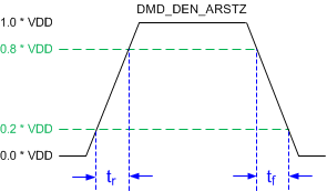 Figure 2. LPSDR Input Rise and Fall Slew Rate
 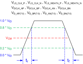 Figure 3. SubLVDS Input Rise and Fall Slew Rate
 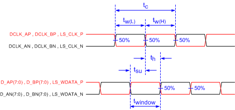 Figure 4. SubLVDS Switching Parameters
 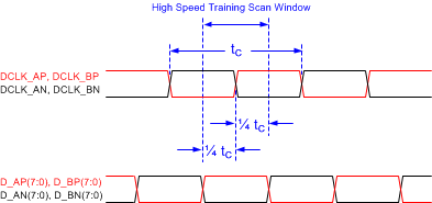 Figure 5. High-Speed Training Scan Window
 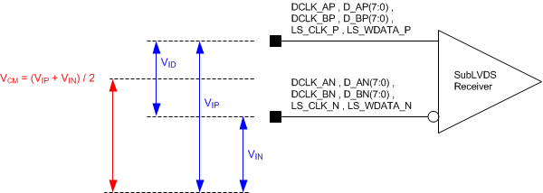 Figure 6. SubLVDS Voltage Parameters
 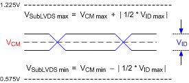 Figure 7. SubLVDS Waveform Parameters
 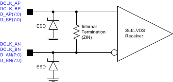 Figure 8. SubLVDS Equivalent Input Circuit
  Figure 9. LPSDR Input Hysteresis