ZHCSJ27 November 2018 DLP650LNIR
PRODUCTION DATA.
- 1 特性
- 2 应用
- 3 说明
- 4 修订历史记录
- 5 Pin Configuration and Functions
-
6 Specifications
- 6.1 Absolute Maximum Ratings
- 6.2 Storage Conditions
- 6.3 ESD Ratings
- 6.4 Recommended Operating Conditions
- 6.5 Thermal Information
- 6.6 Electrical Characteristics
- 6.7 Timing Requirements
- 6.8 System Mounting Interface Loads
- 6.9 Micromirror Array Physical Characteristics
- 6.10 Micromirror Array Optical Characteristics
- 6.11 Window Characteristics
- 6.12 Chipset Component Usage Specification
-
7 Detailed Description
- 7.1 Overview
- 7.2 System Functional Block Diagram
- 7.3
Feature Description
- 7.3.1 DLPC410: Digital Controller for DLP Discovery 4100 Chipset
- 7.3.2 DLPA200: DMD Micromirror Driver
- 7.3.3 DLPR410: PROM for DLP Discovery 4100 Chipset
- 7.3.4 DLP650LNIR: DLP 0.65 WXGA NIR 2xLVDS Series 450 DMD
- 7.3.5 Measurement Conditions
- 7.4 Device Operational Modes
- 7.5 Feature Description
- 7.6 Optical Interface and System Image Quality Considerations
- 7.7 Micromirror Temperature Calculations
- 7.8 Micromirror Landed-On/Landed-Off Duty Cycle
- 8 Application and Implementation
- 9 Power Supply Recommendations
- 10Layout
- 11器件和文档支持
- 12机械、封装和可订购信息
6.4 Recommended Operating Conditions
Over operating free-air temperature range (unless otherwise noted). The functional performance of the device specified in this data sheet is achieved when operating the device within the limits defined by this table. No level of performance is implied when operating the device above or below these limits.| MIN | NOM | MAX | UNIT | ||
|---|---|---|---|---|---|
| VOLTAGE SUPPLY | |||||
| VCC | Supply voltage for LVCMOS core logic(1) | 3.0 | 3.3 | 3.6 | V |
| VCCI | Supply voltage for LVDS Interface(1) | 3.0 | 3.3 | 3.6 | V |
| VCC2 | Micromirror Electrode and HVCMOS voltage(1)(2) | 8.25 | 8.5 | 8.75 | V |
| VMBRST | Micromirror Bias / Reset Voltage(1) | –27 | 26.5 | V | |
| |VCC – VCCI| | Supply voltage delta (absolute value)(3) | 0 | 0.3 | V | |
| LVCMOS INTERFACE | |||||
| VIH | Input High Voltage | 1.7 | 2.5 | VCC + 0.3 | V |
| VIL | Input Low Voltage | –0.3 | 0.7 | V | |
| IOH | High Level Output Current | –20 | mA | ||
| IOL | Low Level Output Current | 15 | mA | ||
| tPWRDNZ | PWRDNZ pulse width(4) | 10 | ns | ||
| SCP INTERFACE | |||||
| ƒSCPCLK | SCP clock frequency(5) | 50 | 500 | kHz | |
| tSCP_PD | Propagation delay, clock to Q, from rising-edge of SCPCLK to valid SCPDO.(6) | 0 | 900 | ns | |
| tSCP_DS | SCPDI clock setup time (before SCPCLK falling-edge)(6) | 800 | ns | ||
| tSCP_DH | SCPDI hold time (after SCPCLK falling-edge)(6) | 900 | ns | ||
| tSCP_NEG_ENZ | Time between falling–edge of SCPENZ and the rising–edge of SCPCLK.(5) | 1 | us | ||
| SCP_POS_ENZ | Time between falling-edge of SCPCLK and the rising–edge of SCPENZ | 1 | us | ||
| tSCP_OUT_EN | Time required for SCP output buffer to recover after SCPENZ (from tri-state). | 192/ƒDCLK | s | ||
| tSCP_PW_ENZ | SCPENZ inactive pulse width (high level) | 1 | 1/ƒscpclk | ||
| tr | Rise Time (20% to 80%). See (6) | 200 | ns | ||
| tf | Fall time (80% to 20%). See (6) | 200 | ns | ||
| LVDS INTERFACE | |||||
| ƒCLOCK | Clock frequency for LVDS interface (all channels), DCLK(7) | 395 | 400 | 405 | MHz |
| |VID| | Input differential voltage (absolute value)(8) | 100 | 400 | 600 | mV |
| VCM | Common mode voltage(8) | 1200 | mV | ||
| VLVDS | LVDS voltage(8) | 0 | 2000 | mV | |
| tLVDS_RSTZ | Time required for LVDS receivers to recover from PWRDNZ | 10 | ns | ||
| ZIN | Internal differential termination resistance | 95 | 105 | Ω | |
| ZLINE | Line differential impedance (PWB/trace) | 90 | 100 | 110 | Ω |
| ENVIRONMENTAL | |||||
| TMIRROR | Micromirror temperature, long–term operational(9)(10)(11) | 10 | 40 to 70(12) | °C | |
| Micromirror temperature, short–term operational(10)(13) | 0 | 10 | °C | ||
| TWINDOW | Window temperature–operational(14) | 10 | 85 | °C | |
| T|DELTA | | Absolute temperature delta between any point on the window edge and the ceramic test point TP1. (15) | 26 | °C | ||
| TDP -AVG | Average dew point temperature (non–condensing)(16) | 28 | °C | ||
| TDP-ELR | Elevated dew point temperature range (non-condensing)(17) | 28 | 36 | °C | |
| CTELR | Cumulative time in elevated dew point temperature range | 24 | Months | ||
| ILLUV | Illumination Power Density < 420 nm(9) | 10 | mW/cm2 | ||
| ILLVIS-NIR | Illumination Power Density between 420 nm and 950 nm | 40 | W/cm2 | ||
| ILLNIR2A | Illumination Total Power between 950 nm and 1150 nm(18) | 160 | W | ||
| ILLNIR2B | Illumination Power Density between 950 nm and 1150 nm(18) | 500 | W/cm2 | ||
| ILLNIR3 | Illumination Power Density between 1150 nm and 2000 nm | 40 | W/cm2 | ||
| ILLIR | Illumination Power Density > 2000 nm | 10 | mW/cm2 | ||
(1) All voltages are referenced to VSS (common ground). VCC, VCCI, VCC2, and VMBRST power supplies are all required for proper DMD operation. VSS must also be connected to common ground.
(2) VCC2 supply transients must fall within specified max voltages.
(3) To prevent excess current, the supply voltage delta |VCCI – VCC| must be less than the specified limit.
(4) PWRDNZ input pin resets the SCP and disables the LVDS receivers. PWRDNZ input pin overrides SCPENZ input pin and tri-states the SCPDO output pin.
(5) The SCP clock is a gated clock. Duty cycle must be 50% ± 10%. SCP parameter is related to the frequency of DCLK.
(6) See Figure 3.
(8) See Figure 6 LVDS Waveform Requirements.
(9) Simultaneous exposure of the DMD to the maximum Recommended Operating Conditions for temperature and UV illumination reduces device lifetime.
(10) The mirror temperatures cannot be measured directly and must be computed analytically from the temperature measured at test point 1 (TP1) shown in Figure 20 and the DMD package and mirror thermal resistances using the Micromirror Temperature Calculations.
(11) Long-term is defined as the usable life of the device.
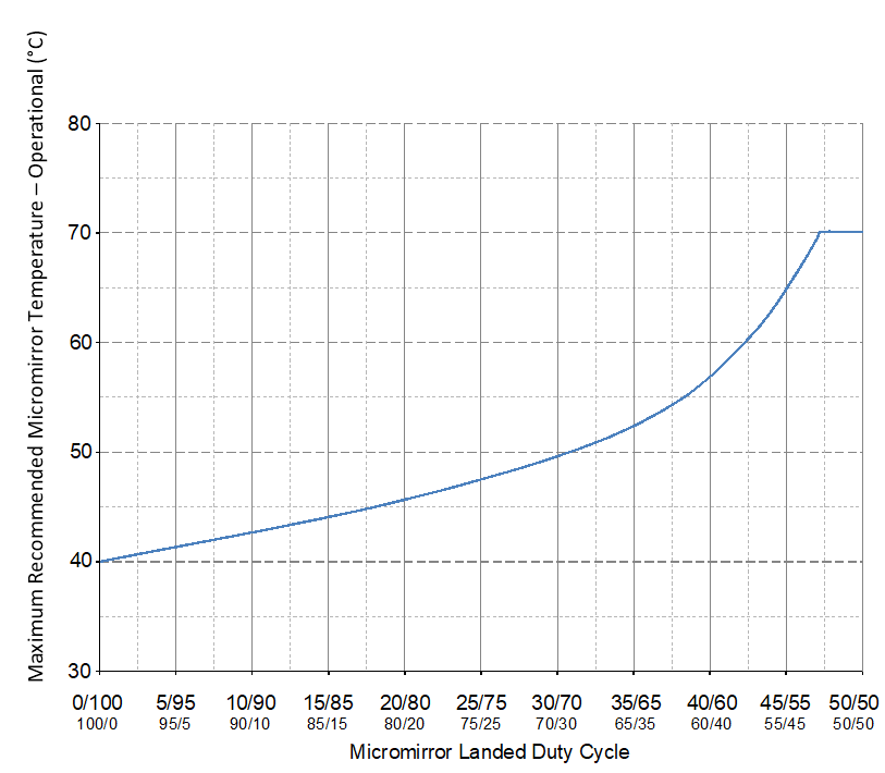
(12) Per Figure 2, derate the maximum operational micromirror temperature based on the micromirror landed duty cycle that the DMD experiences in the end application. See Micromirror Landed-On/Landed-Off Duty Cycle for a definition of micromirror landed duty cycle.
(13) Mirror temperatures beyond those specified as long-term are recommended for short-term conditions only (power-up). Short-term is defined as cumulative time over the usable life of the device and is less than 500 hours.
(14) The locations of thermal test points TP2, TP3, TP4, and TP5 in Figure 20 are intended to measure the highest window edge temperature. For most applications, the locations shown are representative of the highest window edge temperature. If a particular application causes additional points on the window edge to be at a higher temperature, add test points to those locations.
(15) Temperature delta is the highest difference between the ceramic test point 1 (TP1) and anywhere on the window edge as shown in Figure 20. The window test points TP2, TP3, TP4, and TP5 shown in Figure 20 are intended to result in the worst case delta temperature. If a particular application causes another point on the window edge to result in a larger delta temperature, use that point.
(16) The average over time (including storage and operating) that the device is not in the ‘elevated dew point temperature range'.
(17) Limit exposure to dew point temperatures in the elevated range during storage and operation to less than a total cumulative time of CTELR.
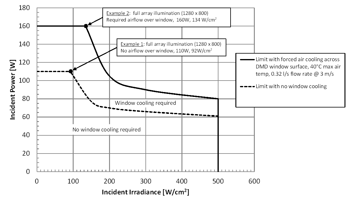
(18) See Figure 1 for allowable combinations of illumination power vs illumination power density. 160W total power is achievable only by full array illumination. 500 W/cm2 is only achievable through partial array illumination. Some combinations of illumination power and power density require cooling of the window with forced air as defined by Figure 1. Refer to the application note DLP® High Power Thermal Design Guide: Focus on High Power NIR Laser Illumination for additional details.
 Figure 1. Maximum Recommended Illumination Incident Power vs Incident Irradiance
  Figure 2. Maximum Recommended Micromirror Temperature - Derating Curve (see Landed Duty Cycle and Operational DMD Temperature)