ZHCSJ27 November   2018 DLP650LNIR

PRODUCTION DATA.  

  1. 特性
  2. 应用
  3. 说明
    1.     Device Images
      1.      简化应用
  4. 修订历史记录
  5. Pin Configuration and Functions
    1.     Pin Functions
  6. Specifications
    1. 6.1  Absolute Maximum Ratings
    2. 6.2  Storage Conditions
    3. 6.3  ESD Ratings
    4. 6.4  Recommended Operating Conditions
    5. 6.5  Thermal Information
    6. 6.6  Electrical Characteristics
    7. 6.7  Timing Requirements
    8. 6.8  System Mounting Interface Loads
    9. 6.9  Micromirror Array Physical Characteristics
    10. 6.10 Micromirror Array Optical Characteristics
    11. 6.11 Window Characteristics
    12. 6.12 Chipset Component Usage Specification
  7. Detailed Description
    1. 7.1 Overview
    2. 7.2 System Functional Block Diagram
    3. 7.3 Feature Description
      1. 7.3.1 DLPC410: Digital Controller for DLP Discovery 4100 Chipset
      2. 7.3.2 DLPA200: DMD Micromirror Driver
      3. 7.3.3 DLPR410: PROM for DLP Discovery 4100 Chipset
      4. 7.3.4 DLP650LNIR: DLP 0.65 WXGA NIR 2xLVDS Series 450 DMD
        1. 7.3.4.1 DLP650LNIR Chipset Interfaces
          1. 7.3.4.1.1 DLPC410 Interface Description
            1. 7.3.4.1.1.1 DLPC410 IO
            2. 7.3.4.1.1.2 Initialization
            3. 7.3.4.1.1.3 DMD Device Detection
            4. 7.3.4.1.1.4 Power Down
          2. 7.3.4.1.2 DLPC410 to DMD Interface
            1. 7.3.4.1.2.1 DLPC410 to DMD IO Description
            2. 7.3.4.1.2.2 Data Flow
          3. 7.3.4.1.3 DLPC410 to DLPA200 Interface
            1. 7.3.4.1.3.1 DLPA200 Operation
            2. 7.3.4.1.3.2 DLPC410 to DLPA200 IO Description
          4. 7.3.4.1.4 DLPA200 to DLP650LNIR Interface
            1. 7.3.4.1.4.1 DLPA200 to DLP650LNIR Interface Overview
      5. 7.3.5 Measurement Conditions
    4. 7.4 Device Operational Modes
      1. 7.4.1 DMD Block Modes
        1. 7.4.1.1 Single Block Mode
        2. 7.4.1.2 Dual Block Mode
        3. 7.4.1.3 Quad Block Mode
        4. 7.4.1.4 Global Mode
      2. 7.4.2 DMD Load4 Mode
    5. 7.5 Feature Description
      1. 7.5.1 Power Interface
      2. 7.5.2 Timing
    6. 7.6 Optical Interface and System Image Quality Considerations
      1. 7.6.1 Optical Interface and System Image Quality
      2. 7.6.2 Numerical Aperture and Stray Light Control
      3. 7.6.3 Pupil Match
      4. 7.6.4 Illumination Overfill
    7. 7.7 Micromirror Temperature Calculations
      1. 7.7.1 Sample Calculation 1: Uniform Illumination of Entire DMD Active Array (1280 × 800 pixels)
      2. 7.7.2 Sample Calculation 2: Partial DMD Active Array Illumination with Non-uniform Illumination Peak
    8. 7.8 Micromirror Landed-On/Landed-Off Duty Cycle
      1. 7.8.1 Definition of Micromirror Landed-On/Landed-Off Duty Cycle
      2. 7.8.2 Landed Duty Cycle and Useful Life of the DMD
      3. 7.8.3 Landed Duty Cycle and Operational DMD Temperature
      4. 7.8.4 Estimating the Long-Term Average Landed Duty Cycle of a Product or Application
  8. Application and Implementation
    1. 8.1 Application Information
      1. 8.1.1 Device Description
    2. 8.2 Typical Application
      1. 8.2.1 Design Requirements
      2. 8.2.2 Detailed Design Procedure
  9. Power Supply Recommendations
  10. 10Layout
    1. 10.1 Layout Guidelines
      1. 10.1.1 Impedance Requirements
      2. 10.1.2 PCB Signal Routing
      3. 10.1.3 Fiducials
      4. 10.1.4 DMD Interface
        1. 10.1.4.1 Trace Length Matching
      5. 10.1.5 DLP650LNIR Decoupling
        1. 10.1.5.1 Decoupling Capacitors
      6. 10.1.6 VCC and VCC2
      7. 10.1.7 DMD Layout
      8. 10.1.8 DLPA200
    2. 10.2 Layout Example
  11. 11器件和文档支持
    1. 11.1 器件支持
      1. 11.1.1 器件命名规则
      2. 11.1.2 器件标记
    2. 11.2 文档支持
      1. 11.2.1 相关文档
    3. 11.3 相关链接
    4. 11.4 接收文档更新通知
    5. 11.5 社区资源
    6. 11.6 商标
    7. 11.7 静电放电警告
    8. 11.8 术语表
  12. 12机械、封装和可订购信息

封装选项

机械数据 (封装 | 引脚)
散热焊盘机械数据 (封装 | 引脚)
订购信息

System Functional Block Diagram

Figure 11 shows a simplified system block diagram with the use of the DLPC410 with the following chipset components:

    DLPC410Xilinx [XC5VLX30] FPGA configured to provide high-speed DMD data and control, and DLPA200 timing and control
    DLPR410 [XCF16PFSG48C] serial flash PROM contains startup configuration information (EEPROM)
    DLPA200 DMD micromirror driver for the DLP650LNIR DMD
    DLP650LNIR Spatial light modulator (DMD)
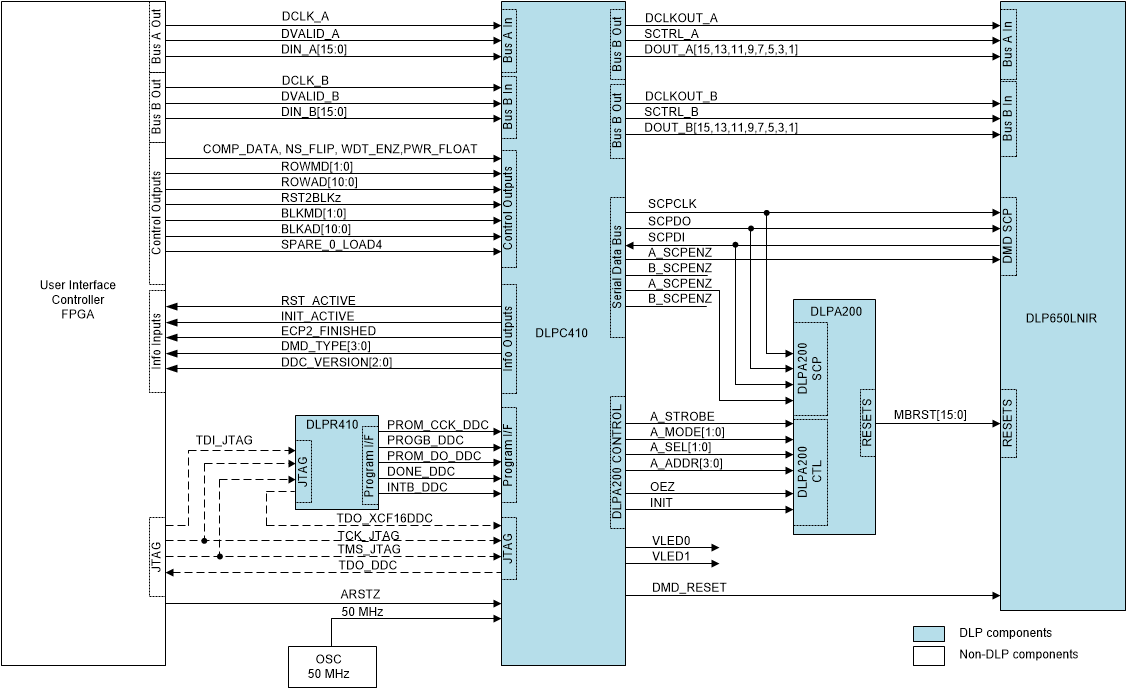
DLP650LNIR sbd-650LNIR-C410-dlps136.gifFigure 11. DLPC410, DLPA200, DLPR410, and DLP650LNIR Functional Block Diagram