ZHCSJ27 November 2018 DLP650LNIR
PRODUCTION DATA.
- 1 特性
- 2 应用
- 3 说明
- 4 修订历史记录
- 5 Pin Configuration and Functions
-
6 Specifications
- 6.1 Absolute Maximum Ratings
- 6.2 Storage Conditions
- 6.3 ESD Ratings
- 6.4 Recommended Operating Conditions
- 6.5 Thermal Information
- 6.6 Electrical Characteristics
- 6.7 Timing Requirements
- 6.8 System Mounting Interface Loads
- 6.9 Micromirror Array Physical Characteristics
- 6.10 Micromirror Array Optical Characteristics
- 6.11 Window Characteristics
- 6.12 Chipset Component Usage Specification
-
7 Detailed Description
- 7.1 Overview
- 7.2 System Functional Block Diagram
- 7.3
Feature Description
- 7.3.1 DLPC410: Digital Controller for DLP Discovery 4100 Chipset
- 7.3.2 DLPA200: DMD Micromirror Driver
- 7.3.3 DLPR410: PROM for DLP Discovery 4100 Chipset
- 7.3.4 DLP650LNIR: DLP 0.65 WXGA NIR 2xLVDS Series 450 DMD
- 7.3.5 Measurement Conditions
- 7.4 Device Operational Modes
- 7.5 Feature Description
- 7.6 Optical Interface and System Image Quality Considerations
- 7.7 Micromirror Temperature Calculations
- 7.8 Micromirror Landed-On/Landed-Off Duty Cycle
- 8 Application and Implementation
- 9 Power Supply Recommendations
- 10Layout
- 11器件和文档支持
- 12机械、封装和可订购信息
7.3.4.1.2.2 Data Flow
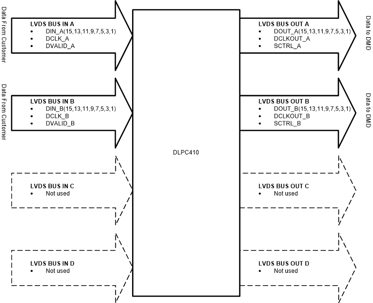
Figure 12 shows the data traffic through the DLPC410. Special considerations are necessary when laying out the DLPC410 to allow best signal flow.
 Figure 12. DLPC410 Data Flow
 Two LVDS buses A and B transfer the data from the user to the DLPC410. Each bus has its own data clock that is input edge aligned with the data (DCLK). Each bus also has its own validation signal that qualifies the data input to the DLPC410 (DVALID).
Output LVDS buses A and B transfer data from the DLPC410 to the DLP650LNIR. The DLP650LNIR uses only the odd input signals of the output buses A and B.
Buses C and D are used with DMDs which have 64-bit wide data inputs only.