ZHCSJ27 November 2018 DLP650LNIR
PRODUCTION DATA.
- 1 特性
- 2 应用
- 3 说明
- 4 修订历史记录
- 5 Pin Configuration and Functions
-
6 Specifications
- 6.1 Absolute Maximum Ratings
- 6.2 Storage Conditions
- 6.3 ESD Ratings
- 6.4 Recommended Operating Conditions
- 6.5 Thermal Information
- 6.6 Electrical Characteristics
- 6.7 Timing Requirements
- 6.8 System Mounting Interface Loads
- 6.9 Micromirror Array Physical Characteristics
- 6.10 Micromirror Array Optical Characteristics
- 6.11 Window Characteristics
- 6.12 Chipset Component Usage Specification
-
7 Detailed Description
- 7.1 Overview
- 7.2 System Functional Block Diagram
- 7.3
Feature Description
- 7.3.1 DLPC410: Digital Controller for DLP Discovery 4100 Chipset
- 7.3.2 DLPA200: DMD Micromirror Driver
- 7.3.3 DLPR410: PROM for DLP Discovery 4100 Chipset
- 7.3.4 DLP650LNIR: DLP 0.65 WXGA NIR 2xLVDS Series 450 DMD
- 7.3.5 Measurement Conditions
- 7.4 Device Operational Modes
- 7.5 Feature Description
- 7.6 Optical Interface and System Image Quality Considerations
- 7.7 Micromirror Temperature Calculations
- 7.8 Micromirror Landed-On/Landed-Off Duty Cycle
- 8 Application and Implementation
- 9 Power Supply Recommendations
- 10Layout
- 11器件和文档支持
- 12机械、封装和可订购信息
7.3.5 Measurement Conditions
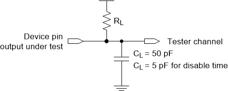
The data sheet provides timing at the device pin. For output timing analysis, the tester pin electronics and its transmission line effects must be taken into account. Figure 14 shows an equivalent test load circuit for the output under test. The load capacitance value stated is only for characterization and measurement of AC timing signals. This load capacitance value does not indicate the maximum load the DMD is capable of driving. All rise and fall transition timing parameters are referenced to VIL(max) and VIH(min) for input clocks, VOL(max) and VOH(min) for output clocks.
 Figure 14. Test Load Circuit for AC Timing Measurements
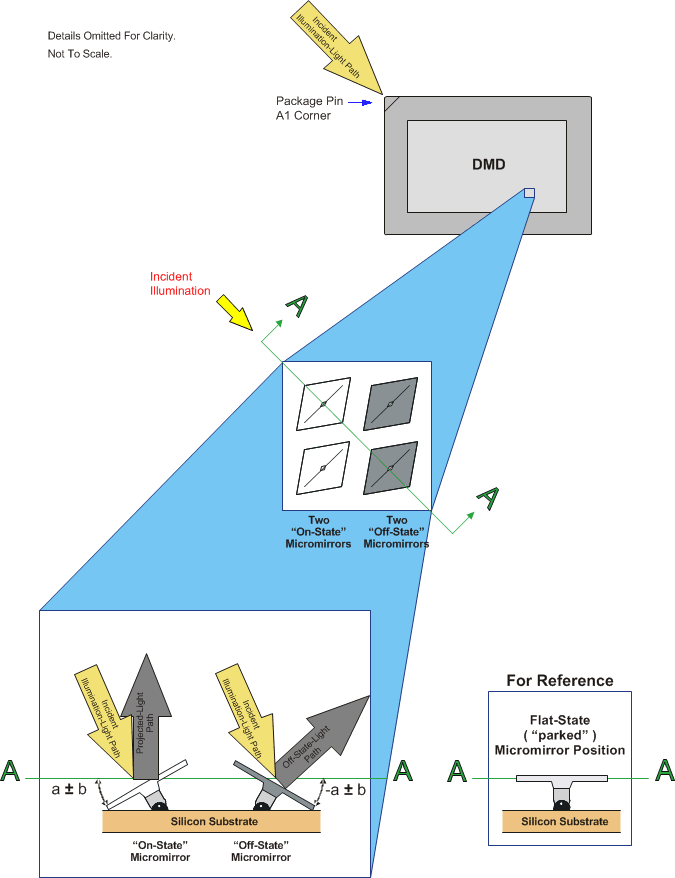
  Figure 15. Micromirror Landed Positions and Light Paths