ZHCSRS7A August 2017 – February 2023 DLP650NE
PRODUCTION DATA
- 1 特性
- 2 应用
- 3 说明
- 4 Revision History
- 5 Pin Configuration and Functions
-
6 Specifications
- 6.1 Absolute Maximum Ratings
- 6.2 Storage Conditions
- 6.3 ESD Ratings
- 6.4 Recommended Operating Conditions
- 6.5 Thermal Information
- 6.6 Electrical Characteristics
- 6.7 Timing Requirements
- 6.8 Window Characteristics
- 6.9 System Mounting Interface Loads
- 6.10 Micromirror Array Physical Characteristics
- 6.11 Micromirror Array Optical Characteristics
- 6.12 Chipset Component Usage Specification
-
7 Detailed Description
- 7.1 Overview
- 7.2 Functional Block Diagram
- 7.3 Feature Description
- 7.4 Device Functional Modes
- 7.5 Optical Interface and System Image Quality Considerations
- 7.6 Micromirror Array Temperature Calculation
- 7.7 Micromirror Landed-On or Landed-Off Duty Cycle
- 8 Power Supply Requirements
- 9 Device Documentation Support
- 10Mechanical, Packaging, and Orderable Information
6.7 Timing Requirements
Over Recommended
Operating Conditions (Section 6.4)
unless otherwise noted.(5)
| DESCRIPTION(1) | MIN | TYP | MAX | UNIT | |||
|---|---|---|---|---|---|---|---|
| SCP INTERFACE(2) | |||||||
| tr | Rise time | 20% to 80% reference points | 200 | ns | |||
| tƒ | Fall time | 80% to 20% reference points | 200 | ns | |||
| LVDS INTERFACE(2) | |||||||
| tr | Rise time | 20% to 80% | 100 | 400 | ps | ||
| tƒ | Fall time | 80% to 20% | 100 | 400 | ps | ||
| LVDS CLOCKS(3) | |||||||
| tc | Cycle time | DCLK_A, 50% to 50% | 2.5 | ns | |||
| DCLK_B, 50% to 50% | 2.5 | ||||||
| tw | Pulse duration | DCLK_A, 50% to 50% | 1.19 | 1.25 | ns | ||
| DCLK_B, 50% to 50% | 1.19 | 1.25 | |||||
| LVDS INTERFACE(3) | |||||||
| tsu | Setup time | D_A(15:0) before rising or falling edge of DCLK_A | 0.1 | ns | |||
| D_B(15:0) before rising or falling edge of DCLK_B | 0.1 | ||||||
| tsu | Setup time | SCTRL_A before rising or falling edge of DCLK_A | 0.1 | ns | |||
| SCTRL_B before rising or falling edge of DCLK_B | 0.1 | ||||||
| th | Hold time | D_A(15:0) after rising or falling edge of DCLK_A | 0.4 | ns | |||
| D_B(15:0) after rising or falling edge of DCLK_B | 0.4 | ||||||
| th | Hold time | SCTRL_A after rising or falling edge of DCLK_A | 0.3 | ns | |||
| SCTRL_B after rising or falling edge of DCLK_B | 0.3 | ||||||
| LVDS INTERFACE(4) | |||||||
| tskew | Skew time | Channel B relative to Channel A(4) | Channel A includes the following LVDS pairs: DCLK_AP and DCLK_AN SCTRL_AP and SCTRL_AN D_AP(15:0) and D_AN(15:0) | –1.25 | 1.25 | ns | |
| Channel B includes the following LVDS pairs: DCLK_BP and DCLK_BN SCTRL_BP and SCTRL_BN D_BP(15:0) and D_BN(15:0) | |||||||
(1) Refer to Section 5 for pin details.
(2) Refer to Figure 6-6.
(3) Refer to Figure 6-8.
(4) Refer to Figure 6-9.
(5) Tested at the device pin. For output timing analysis, the tester pin
electronics and its transmission line effects must
be
considered.
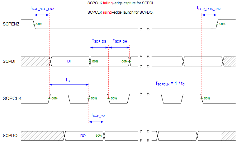
Not to scale
Refer to
the
SCP Interface section of the
Recommended
Operating Conditions
Section 6.4.
Figure 6-2 SCP Timing Parameters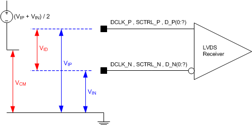
Refer to
the
LVDS Interface section of the
Recommended
Operating Conditions (Section 6.4).
Refer to the
Pin
Functions
table
for the list of LVDS pins.
Figure 6-3 LVDS Voltage Definitions (References)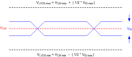
Not to scale
Refer to
the
LVDS Interface section of the
Recommended
Operating Conditions (Section 6.4).
Figure 6-4 LVDS Voltage Parameters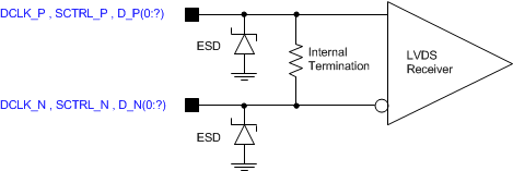
Refer to
the
LVDS Interface section of the
Recommended
Operating Conditions (Section 6.4).
Refer to the Pin Functions
table
for
the
list of LVDS pins.
Figure 6-5 LVDS Equivalent Input Circuit
Not to scale
Refer to the timing
requirements.
Refer to
the
Pin Functions table for
the
list of LVDS pins and SCP pins.
Figure 6-6 Rise Time and Fall Time Figure 6-7 Test Load Circuit for Output Propagation Measurement
For output timing analysis, the tester pin electronics and its transmission line effects must be considered. System design should use IBIS or other simulation tools to correlate the timing reference load to a system environment. See Figure 6-7.
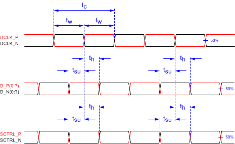
Not to scale
Refer to
the
LVDS
Interface
section in the timing requirements.
Figure 6-8 Timing Requirement Parameter Definitions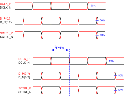
Not to scale
Refer to
the
LVDS
Interface
section in the timing requirements.
Figure 6-9 LVDS Interface Channel Skew Definition