ZHCSKV8A November 2020 – June 2022 DLP670S
PRODUCTION DATA
- 1 特性
- 2 应用
- 3 说明
- 4 Revision History
- 5 Pin Configuration and Functions
-
6 Specifications
- 6.1 Absolute Maximum Ratings
- 6.2 Storage Conditions
- 6.3 ESD Ratings
- 6.4 Recommended Operating Conditions
- 6.5 Thermal Information
- 6.6 Electrical Characteristics
- 6.7 Capacitance at Recommended Operating Conditions
- 6.8 Timing Requirements
- 6.9 Typical Characteristics
- 6.10 System Mounting Interface Loads
- 6.11 Micromirror Array Physical Characteristics
- 6.12 Micromirror Array Optical Characteristics
- 6.13 Window Characteristics
- 6.14 Chipset Component Usage Specification
- 7 Detailed Description
- 8 Application and Implementation
- 9 Power Supply Recommendations
- 10Layout
- 11Device and Documentation Support
- 12Mechanical, Packaging, and Orderable Information
6.12 Micromirror Array Optical Characteristics
Table 6-4 Micromirror Array Optical Characteristics
| PARAMETER | TEST CONDITION | MIN | NOM | MAX | UNIT |
|---|---|---|---|---|---|
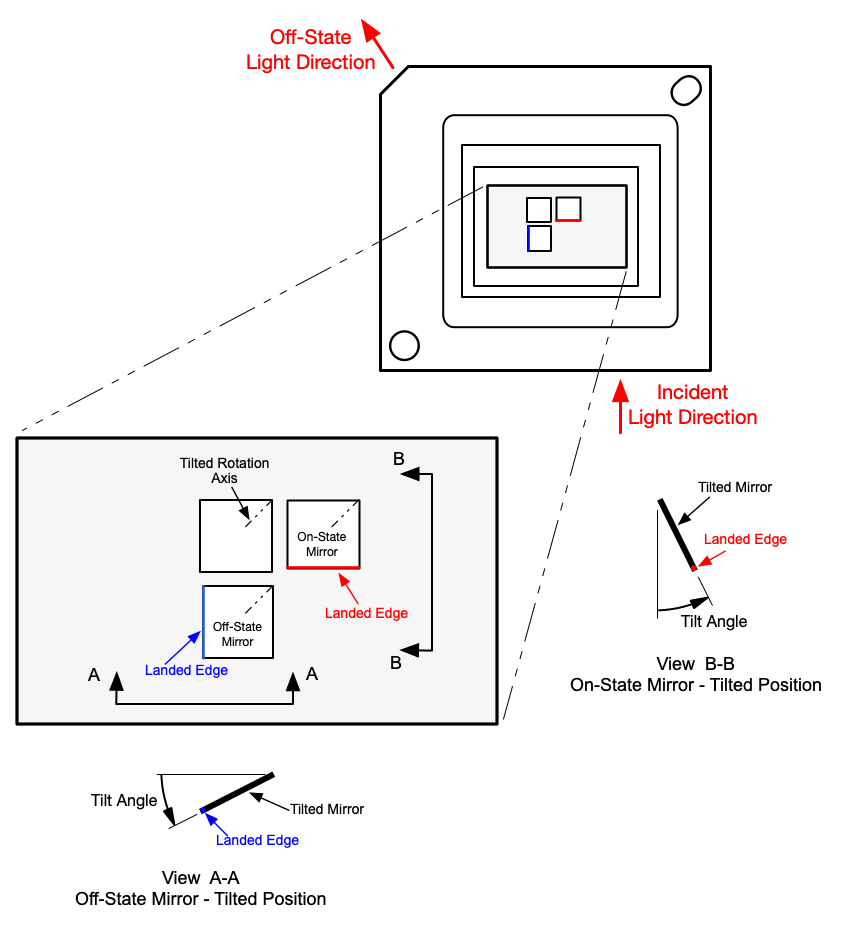
| Mirror tilt angle (1)(2)(3)(4) | Landed State | 15.6 | 17.5 | 18.4 | degrees |
| Micromirror crossover time (5) | Typical Performance | 1 | 3 | µS | |
| Micromirror switching time (6) | Typical Performance | 10 | |||
| Number of out-of-specification micromirrors (7) | Adjacent micromirrors | 0 | micromirrors | ||
| Non-Adjacent micromirrors | 10 | ||||
| DMD Photopic Efficiency(8) | 420 nm – 700 nm | 65% |
(1) Measured relative to the plane formed by the overall micromirror array
(2) Represents the variation that can occur between any two individual micromirrors, located on the same device or located on different devices.
(3) For some applications, it is critical to account for the micromirror tilt angle
variation in the overall system optical design. With some system optical designs, the
micromirror tilt angle variation within a device may result in perceivable
nonuniformities
in the light field reflected from the micromirror array. With some system optical designs,
the micromirror tilt angle variation between devices may result in colorimetry variations,
system efficiency variations, system contrast variations, and optical power
variations.
(4) When the micromirror array is landed (not parked), the tilt direction of each
individual micromirror is dictated by the binary contents of the CMOS memory cell
associated with each individual micromirror. A binary value of 1 results in a micromirror
landing in the ON State direction. A binary value of 0 results in a micromirror landing in
the OFF State direction. See Figure 6-10.
(5) The time required for a micromirror to nominally transition from one landed state to the opposite landed state.
(6) The minimum time between successive transitions of a micromirror.
(7) An out-of-specification micromirror is defined as a micromirror that is unable
to transition between the two landed states within the specified
micromirror
switching
time.
(8) Efficiency numbers assume 35-degree illumination angle, F/2.4 illumination and
collection cones, uniform source spectrum, and uniform pupil
illumination.
- Window Transmission 94% (double Pass, Through Two Window Surfaces)
- Micromirror Reflectivity 88%
- Array Diffraction Efficiency 84% (@f/2.4)
- Array Fill Factor 93%
 Figure 6-10 Micromirror Landed Orientation and Tilt