DLPS036B September 2014 – October 2016 DLP9000
PRODUCTION DATA.
- 1 Features
- 2 Applications
- 3 Description
- 4 Revision History
- 5 Description (continued)
- 6 Pin Configuration and Functions
-
7 Specifications
- 7.1 Absolute Maximum Ratings
- 7.2 Storage Conditions
- 7.3 ESD Ratings
- 7.4 Recommended Operating Conditions
- 7.5 Thermal Information
- 7.6 Electrical Characteristics
- 7.7 Timing Requirements
- 7.8 Capacitance at Recommended Operating Conditions
- 7.9 Typical Characteristics
- 7.10 System Mounting Interface Loads
- 7.11 Micromirror Array Physical Characteristics
- 7.12 Micromirror Array Optical Characteristics
- 7.13 Optical and System Image Quality
- 7.14 Window Characteristics
- 7.15 Chipset Component Usage Specification
- 8 Parameter Measurement Information
- 9 Detailed Description
- 10Application and Implementation
- 11Power Supply Requirements
- 12Layout
- 13Device and Documentation Support
- 14Mechanical, Packaging, and Orderable Information
13 Device and Documentation Support
13.1 Device Support
13.1.1 Device Handling
All external signals on the DMD are protected from damage by electrostatic discharge, and are tested in accordance with JESD22-A114-B electrostatic discharge (ESD) sensitivity testing human body model (HBM).
Table 10. DMD ESD Protection Limits
| PACKAGE TERMINAL TYPE | VOLTAGE (MAXIMUM) | UNIT |
|---|---|---|
| Input | 2000 | V |
| Output | 2000 | V |
| VCC | 2000 | V |
| VCCI | 2000 | V |
| VOFFSET | 2000 | V |
| VBIAS | 2000 | V |
| VRESET | 2000 | V |
| All MBRST | 2000 | V |
All CMOS devices require proper Electrostatic Discharge (ESD) handling procedures. Refer to drawing 2504641 DMD Handling Specification, for precautions to protect the DMD from ESD and to protect the DMD’s glass and electrical contacts. Refer to drawing 2504640 DMD Glass Cleaning Procedure, for correct and consistent methods for cleaning the glass of the DMD, in such a way that the anti-reflective coatings on the glass surface are not damaged.
13.1.2 Device Nomenclature
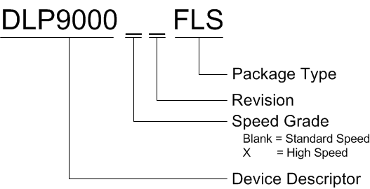
Figure 21 provides a legend for reading the complete device name for any DLP device.
Table 11. Package-Specific Information
| PACKAGE TYPE | ALTERNATE NAME |
|---|---|
| FLS | LCCC |
 Figure 21. Device Nomenclature
13.1.3 Device Markings
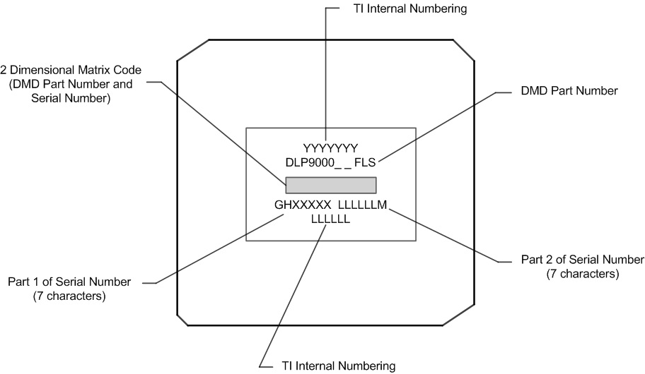
The device marking will include both human-readable information and a 2-dimensional matrix code. The human-readable information is described in Figure 22. The 2-dimensional matrix code is an alpha-numeric character string that contains the DMD part number, Part 1 of Serial Number, and Part 2 of Serial Number. The first character of the DMD Serial Number (part 1) is the manufacturing year. The second character of the DMD Serial Number (part 1) is the manufacturing month. The last character of the DMD Serial Number (part 2) is the bias voltage bin letter.
 Figure 22. DMD Markings
13.2 Documentation Support
13.2.1 Related Documentation
The following documents contain additional information related to the use of the DLP9000 family of devices:
13.3 Community Resources
The following links connect to TI community resources. Linked contents are provided "AS IS" by the respective contributors. They do not constitute TI specifications and do not necessarily reflect TI's views; see TI's Terms of Use.
-
TI E2E™ Online Community TI's Engineer-to-Engineer (E2E) Community. Created to foster collaboration among engineers. At e2e.ti.com, you can ask questions, share knowledge, explore ideas and help solve problems with fellow engineers.
-
Design Support TI's Design Support Quickly find helpful E2E forums along with design support tools and contact information for technical support.
13.4 Trademarks
E2E is a trademark of Texas Instruments.
DLP is a registered trademark of Texas Instruments.
All other trademarks are the property of their respective owners.
13.5 Electrostatic Discharge Caution

These devices have limited built-in ESD protection. The leads should be shorted together or the device placed in conductive foam during storage or handling to prevent electrostatic damage to the MOS gates.
13.6 Glossary
SLYZ022 — TI Glossary.
This glossary lists and explains terms, acronyms, and definitions.