ZHCSFY9 February 2017 DLPA100
PRODUCTION DATA.
- 1 特性
- 2 应用
- 3 说明
- 4 修订历史记录
- 5 Pin Configuration and Functions
- 6 Specifications
-
7 Detailed Description
- 7.1 Overview
- 7.2 Functional Block Diagram
- 7.3 Feature Description
- 7.4 Device Functional Modes
- 8 Application and Implementation
- 9 Power Supply Recommendations
- 10Layout
- 11器件和文档支持
- 12机械、封装和可订购信息
10 Layout
10.1 Layout Guidelines
The 12-V supply, VBB, should be provided on a separate plane, or portion of a shared power distribution plane. Each ceramic filter capacitor should be placed as close as possible to each VBB terminal: pins 9, 22, 37 and 42. The additional reservoir capacitor should also be placed as close as possible to the VBB terminals. The ground for VBB should be routed directly to the DLPA100 thermal pad connection.
The PWB traces used on the switching regulators should be as short and wide as possible. The electrical loops formed between the VBB filter capacitors, input switch (LX pins), inductor, output capacitor and the diode should be as small as possible.
An adjacent layer ground region covering the entire switching node should be provided for the pins: LXC (pin 25), LX5 (pin 23), LX33 (pin 43), LX25 (pin 41), and VMSW (pin10). Each of the switching nodes and all associated components should be located as near the DLPA100 device as possible.
Avoid routing any noise sensitive signals near the DLPA100 device switching nodes and associated ground regions. The sensitive pins on the DLPA100 device consist of pins 1, 2, 3, 4, 5, 6, 8, and 48. If sensitive signals must be routed across the switching loops, use subdivided planes and/or multiple ground planes to avoid interference. Use of shielded inductors on the switching regulator circuits will minimize the possibility of crosstalk and interference.
High current paths should have an adequate number of vias to minimize resistance and inductance. Placement and routing priority should be given to the higher current circuits. For example, the VCORE supply should take precedence over a fan PWM output. The following is the order of precedence from highest to lowest:
- VCORE
- V5
- V3P3
- V2P5
- VM
- VLIN2
- VLIN1
- FAN1, FAN2, FAN3
Suitable kelvin connections should be provided for the regulator feedback pins: FBC (pin 30), V2P5 (pin 46), V3P3 (pin 45), V5 (pin 24), FB1 (pin 31) & FB2 (pin 32) and for sense pins: SENSE (pin 14), ISEN (pin 28) & ISENK (pin 27). Also note that the external feedback networks used for the VCORE and VLIN1 regulators should also deploy kelvin connections. The feedback pin traces FBC, FB1, FB2 are most prone to interference and should be located near the DLPA100 device.
10.2 Grounding Guidelines
Ground pin 19 is isolated internally to the DLPA100 from pins 7 and 44. All three ground pins should be tied together on the PWB at the DLPA100 thermal pad connection. Depending on the application there are three grounding approaches for board layout:
- Completely isolated ground regions for the DLPA100 subcircuits.
- Single isolated ground region for the collective DLPA100 circuit.
- Non-isolated common ground region for the entire board.
The most favorable approach should be carefully considered for the specific application.
10.2.1 Completely Isolated Ground Regions
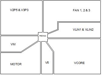
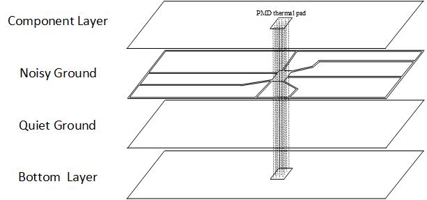
In this case, the PWB has an isolated ground layer around the DLPA100 circuit which serves as a “noisy” ground for the motor driver, switchers, and linear regulators. This plane can be subdivided into isolated sections around each switcher, linear regulator and motor block to minimize the possibility of noise crosstalk between the regulator circuits. See Figure 6. Each isolated section should be connected in a “star” configuration at the DLPA100 thermal pad position. An additional “quiet” solid ground plane should be provided on a separate layer for reference to the sensitive blocks of the DLPA100 device and other sensitive external circuitry. The sensitive pins on the DLPA100 device are pins 1, 2, 3, 4, 5, 6, 8, and 48. The quiet ground plane should connect to the DLPA100 device with the array of thermal vias.
 Figure 6. Noisy Ground Layer
 Figure 7. PWB Planes
10.2.2 Single Isolated Ground Region
In this case, the PWB has a single isolated ground layer around the DLPA100 circuit. This ground layer serves as a “noisy” ground for the switchers, linear regulators, and motor driver. An additional “quiet” solid ground plane should be provided on a separate layer for reference to the sensitive blocks of the DLPA100 and other sensitive external circuitry. Connect the “quiet” and “noisy” ground planes at the DLPA100 thermal pad array of vias.
10.2.3 Non-isolated Common Ground Region
In this case, the PWB has a solid non-isolated common ground layer for the entire board. In this configuration, use particular care during component placement and separate the noisy portions of the DLPA100 circuit from other sensitive signals on the board. The ground plane should connect to the DLPA100 with the array of thermal vias.
10.3 Thermal Guidelines
The PWB should have a thermal pad underneath the DLPA100 on both the top and bottom layers. The thermal pad on the top layer should extend to the edge of the terminal pads and include a 4x4 array of thermal vias. These thermal pads should connect to the internal ground planes via the thermal vias. It is recommended that the internal ground plane should extend for at least 20 square inches.
Careful consideration should be taken in providing an adequate amount of copper traces around the discrete Schottky diodes and MOSFET terminals used in the switching and linear converters to ensure proper thermal management. The thermal impedance (Tj-a) of each component should be calculated to determine the corresponding amount of copper required. If using an internal plane, it is important to use an array of thermal vias underneath the device tab or terminal to assist in the transfer of the heat.
10.4 Motor Control Guidelines
The DLPA100 motor control terminals should be filtered with voltage transient suppressing devices for improved startup reliability and noise immunity. Schottky diodes should be placed cathode to anode between VBB to motor terminals OUTA (pin 12), OUTB (pin 15), OUTC (pin 16) and CTAP (pin 13). Schottky diodes should also be placed cathode to anode between motor terminals OUTA (pin 12), OUTB (pin 15), OUTC (pin 16) and CTAP (pin 13) to ground. Series RC snubbers consisting of a capacitor (0.001 μF) in series with a resistor (150 Ω) should be placed between the motor terminals OUTA (pin12), OUTB (pin 15), and OUTC (pin 16) to CTAP (pin 13).
The value of the motor current sensing resistor on SENSE (pin 14) should be thoroughly evaluated for the application. Careful consideration should be taken in the amount of current draw during motor startup and braking with respect to the speed range and speed change timing requirements. It is recommended that the SENSE (pin 14) voltage does not exceed 450 mV. Most motors from today’s modern technology have relatively low operating currents but higher start-up currents which make it very difficult to achieve good signal to noise ratio during operating range and meet the 450 mV maximum on SENSE (pin 14). Most motors have demonstrated success well below 100 mV steady-state SENSE (pin 14) voltage. As long as good layout and component selection practices are followed, acceptable signal to noise ratios can be achieved at such low operating SENSE (pin 14) voltages. The typical SENSE resistor value ranges from 0.47 Ω to 2.2 Ω. A 1.0-Ω SENSE resistor value is suggested as a good starting point. Typically the steady-state SENSE (pin 14) voltage with a 1.0-Ω resistor will be near 100 mV.
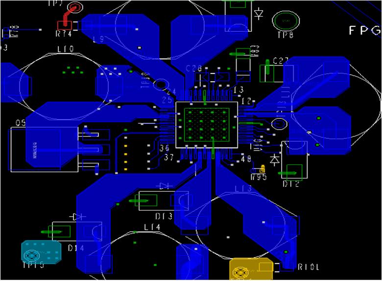
10.5 Layout Example
 Figure 8. Top Layer