ZHCSFY9 February 2017 DLPA100
PRODUCTION DATA.
- 1 特性
- 2 应用
- 3 说明
- 4 修订历史记录
- 5 Pin Configuration and Functions
- 6 Specifications
-
7 Detailed Description
- 7.1 Overview
- 7.2 Functional Block Diagram
- 7.3 Feature Description
- 7.4 Device Functional Modes
- 8 Application and Implementation
- 9 Power Supply Recommendations
- 10Layout
- 11器件和文档支持
- 12机械、封装和可订购信息
7 Detailed Description
7.1 Overview
The DLPA100 is a power management and motor driver IC optimized for DLP video and data display systems and meant for use in either embedded or accessory projector applications. DLPA100 is part of the chipset comprising of the DLP660TE DMD and DLPC4422 controller.
7.2 Functional Block Diagram

7.3 Feature Description
7.3.1 Power Up Sequencing
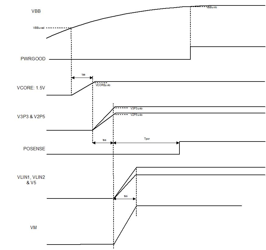
Once the VBB voltage reaches the VBBuvsd threshold (specification defined in Shutdown), the VCORE channel soft-starts within a period of 5 ms typical (tss). Once this period is completed and the VCOREuvlo has been reached, the V3P3 and V2P5 rails soft-start, ramping up ratiometrically. Once each of the three rails are above their respective undervoltage lockout levels (VCOREuvlo, V3P3uvlo, V2P5uvlo), the POSENSE flag will go high after a period of 150 ms typical (Tpor) and also, the VLIN1, VLIN2, V5 and VM rails soft-start, ramping up ratiometrically. Note that VLIN1, VLIN2, V5 and VM can be individually disabled via the serial port, although VLIN1 and VLIN2 require V5 to be present.
The PWRGOOD flag will go high once the POSENSE is high and the VBB voltage is above the undervoltage lockout threshold VBBuvlo.
 Figure 1. Power Up Sequencing Timing Diagram
7.3.2 Power Down Sequencing
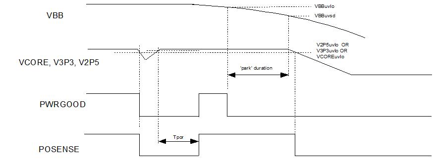
If VBB drops below the undervoltage level (VBBuvlo), the PWRGOOD will flag. If VBB drops below the undervoltage level (VBBuvsd), all the switcher and linear channels will turn off and the output rails will be supplied by the output filter capacitors. The duration between VBBuvlo and VBBuvsd allows sufficient ‘hold up’ time to ‘park’ the DMD mirrors. Although the regulators can supply rated current down to VBBuvsd, they can only provide this power for a maximum of 0.5 ms.
If either of the rails: VCORE or V3P3 or V2P5 drop below their respective undervoltage levels, the POSENSE and PWRGOOD will flag immediately.
 Figure 2. Power Down Sequencing Timing Diagram
7.3.3 Shutdown
In the event of a fault either due to excessive junction temperature, or low voltage on VCP, or low voltage on VREG, or low VBB voltage, each switcher and linear channel is disabled.
A low VBB voltage, VBBuvsd in this case, shuts down the DLPA100, protecting it from excessive power dissipation. An undervoltage power monitoring flag, PWRGOOD is also provided, to indicate when the VBB voltage is operating in and out of normal operating range.
7.3.3.1 Thermal
An overtemperature monitor provides a warning when the junction temperature reaches 130°C. The DLPA100 is protected from excessive temperatures by an internal circuit that will shut the device down immediately the junction temperature reaches 165°C. As soon as the temperature drops below the hysteresis level, the regulators will start-up again under soft-start control, assuming all other conditions are met (VCP, VBB etc.).
7.3.4 System Reset
The DLPA100 device can be reset by using the RESETZ input. This feature can be used during start-up conditions to reset the serial port registers to a known set of states. It can also be used during power-down conditions to disable certain features before complete shutdown occurs. The DLPC4422 display controller software controls which functions are reset to the power on reset (POR) state when RESETZ is initiated.
- MSKFAN: Masks the reset of the 3 fan drivers (POR state = disabled, PWM=0%).
- MSKREG: Masks the reset of linear regulators VLIN1 & VLIN2, and 5V switcher (POR state = enabled).
- MSKMOT: Masks the reset of the motor controller configuration registers (POR state = 0).
- MSKMOTE: Masks the reset of the motor controller output enable bit (POR state = disabled).
7.3.5 Interrupt Logic
PMDINTZ is an active low open drain output that will be asserted if the DLPA100 goes into thermal shutdown at 165°C. The open drain output is held low by using the DLPA100 internal regulator even though the rest of the DLPA100 device is shut down. This internal regulator only depends on 12 V being operational to allow retention of the data in the latched status registers if any of the supplies are lost. PMDINTZ is primarily used as an interrupt to the DLP controller but can also be used to drive an LED overtemp indicator on the projector.
The thermal warning signal (TWARN) can also trigger an interrupt if enabled. Over-current events for the three DLP controller supplies can also cause PMDINTZ to go low. The DLP controller processor can clear or set PMDINTZ by writing to the latches that capture the interrupts. The DLP controller can also mask any of the interrupts (except TSD) via the enable interrupt register.
The raw status register can be read back in real time to monitor the fault condition. If the faults are present for a valid time, they will be latched into the latched status register.
7.3.6 Serial Communications Port
The Serial communications port (SCP) is a full duplex, synchronous, character-oriented byte port that allows exchange of data between the DLP controller (master) and the DLPA100.
Table 1. Serial Communications Port Signal Definitions
| SIGNAL | I/O | FROM/TO | TYPE | DESCRIPTION |
|---|---|---|---|---|
| SCPK | I | SCP bus master to slave | LVTTL compatible | SCP bus serial transfer clock. The host processor (master) generates this clock. |
| SCPENZ | I | SCP bus master to slave | LVTTL compatible | SCP bus access enable (low true). When high, slave will reset to idle state, and SCPDO output will tri-state. Pulling SCPENZ low initiates a read or write access. SCPENZ must remain low for an entire read/write access, and must be pulled high after the last data cycle. To abort a read or write cycle, pull SCPENZ high at any point. |
| SCPDI | I | SCP bus master to slave | LVTTL compatible | SCP bus serial data input. Data bits are valid and must be clocked in on the falling edge of SCPCK. |
| SCPDO | O | SCP bus slave to master | LVTTL open drain w/tri-state | SCP bus serial data output. Data bits must clocked out on the rising edge of SCPCK. |
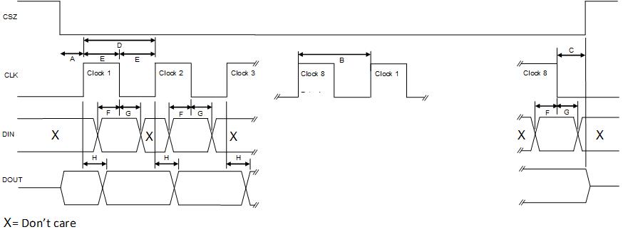
Table 2. Serial Interface Timing Requirements
| SYMBOL | CHARACTERISTICS | TEST CONDITIONS | MIN | NOM | MAX | UNIT |
|---|---|---|---|---|---|---|
| A | Setup CSZ low to CLK | Reference to rising edge of CLK | 360 | ns | ||
| B | Byte to Byte Delay | Nominally 1 CLK cycle rising edge to rising edge | 1.9 | µs | ||
| C | Setup DIN to CSZ High | Last byte to slave disable | 360 | ns | ||
| CLK Frequency | 0 | 526 | kHz | |||
| D | CLK Period | 1.9 | 2 | µs | ||
| E | CLK High or Low Time | 300 | ns | |||
| F | DIN Set-Up Time | Reference to falling edge of CLK | 300 | ns | ||
| G | DIN Hold Time | Reference from falling edge of CLK | 300 | ns | ||
| H | DOUT Propogation Delay | Reference from rising edge of CLK | 300 | ns | ||
| CLK Filter (pulse reject) | 200 | ns |
 Figure 3. Serial Communications Port Timing Diagram
7.3.7 Switching Regulators
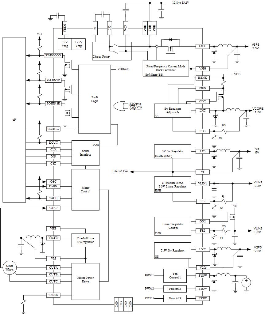
The DLPA100 has four fixed frequency current mode control buck regulators that are used to provide power to integrated circuits in the system. The V5 regulator is used to power control functions in the DLPA100, as well as power the VLIN1 and VLIN2 linear regulators.
The regulators require external fly back diodes, inductors and filter capacitors. Due to the high currents in the VCORE regulator, an external FET and sense resistor are required. The regulators will operate in both continuous and discontinuous mode. An internal blanking circuit will be used to filter out transients due to the reverse recovery of the external clamp diode.
7.3.7.1 Output Voltage - VOUT
All of the switchers apart from VCORE are regulated with respect to a 1.2 V reference (VFB). As the Core Regulator (VCORE) output voltage is adjustable from 1.0 V to 3.3 V the internal reference for this output is 0.8 V.
7.3.7.2 Adjustable Linear Regulator - VLIN1
This low dropout type regulator features current limit for a shorted load. It includes an integrated n-channel pass element and can work with either ceramic or electrolytic output capacitors. The output can range between 1.0 V and 3.3 V. The output voltage of the adjustable regulator is set by:
where
- VFB= 0.8 V
7.3.7.3 Adjustable Linear Regulator Control - VLIN2
An additional linear regulator is implemented with external n-channel pass element. The output can range between 1.0 V and 3.3 V. The output voltage of the adjustable regulator is set by:
where
- VFB= 0.8 V
7.3.8 Fan Controllers
The DLPA100 has three outputs available to be used as the switching node for either voltage mode step down switcher or ‘direct drive’ schemes. The output voltage is determined by a PWM value programmed using the DLPC4422 display controller software. The switching frequency for each output can be programmed using the DLPC4422 display controller software for either 100 kHz for applications requiring a step-down switcher, or 24 Hz in applications that can utilize a direct drive scheme. The drivers in the ‘direct drive’ scheme are connected to the corresponding fans via a series resistor.
The default condition at start-up will be separate control of each fan control channel and 100kHz switching frequency.
7.3.9 Color Wheel Motor Driver
The driver system is a three phase BEMF sensing motor controller and driver. Commutation is controlled by a proprietary BEMF sensing technique. It eliminates many external passive components and provides flexibility by allowing various timing parameters to be programmed via the serial port.
7.3.9.1 Color Wheel Motor Driver Power Dissipation
The maximum allowable power dissipation on motor driver is specified in the color wheel motor driver table. Motor driver power dissipation can be calculated as follows:
where
- Pdm = Power dissipation of motor driver
- VM = Programmed output voltage of the motor supply
- KE = Motor voltage constant in Volts/(rad/sec)
- Sm = Motor speed in rad/sec
- Ispd = Motor current at Sm speed
- Rpp = Phase-to-phase motor resistance
7.3.10 Color Wheel Switching Regulator Supply
A fixed off time switching regulator is included to manage power dissipation for driving color wheels. For highly resistive motors requiring a low running current, Irun < 75 mA, using this regulator may not be required, in which case VM should be connected directly to VBB and the external inductor, capacitor & Schottky diode do not need to be fitted.
7.4 Device Functional Modes
DLPA100 device functional modes are controlled by the DLPC4422 display controller. See the DLPC4422 display controller datasheet or contact a TI applications engineer.