ZHCSCO5B June 2014 – February 2018 DLPA2000
PRODUCTION DATA.
- 1 特性
- 2 应用
- 3 说明
- 4 修订历史记录
- 5 Pin Configuration and Functions
- 6 Specifications
-
7 Detailed Description
- 7.1 Overview
- 7.2 Functional Block Diagram
- 7.3
Feature Description
- 7.3.1 DMD Regulators
- 7.3.2 RGB Strobe Decoder
- 7.3.3 LED Current Control
- 7.3.4 Calculating Inductor Peak Current
- 7.3.5 LED Current Accuracy
- 7.3.6 Transient Current Limiting
- 7.3.7 1.1-V Regulator (Buck Converter)
- 7.3.8 Motor Driver
- 7.3.9 Measurement System
- 7.3.10
Protection Circuits
- 7.3.10.1 Thermal Warning (HOT) and Thermal Shutdown (TSD)
- 7.3.10.2 Low Battery Warning (BAT_LOW) and Undervoltage Lockout (UVLO)
- 7.3.10.3 DMD Regulator Fault (DMD_FLT)
- 7.3.10.4 V6V Power-Good (V6V_PGF) Fault
- 7.3.10.5 VLED Overvoltage (VLED_OVP) Fault
- 7.3.10.6 VLED Power Save Mode
- 7.3.10.7 V1V8 PG Failure
- 7.3.10.8 Interrupt Pin (INTZ)
- 7.3.10.9 SPI
- 7.3.11 Password Protected Registers
- 7.4 Device Functional Modes
- 7.5
Register Maps
- Table 7. Register Description
- 7.5.1 Chip Revision Register
- 7.5.2 Enable Register
- 7.5.3 Transient-Current Limit Settings
- 7.5.4 Regulation Current MSB, SW4
- 7.5.5 Regulation Current LSB, SW4
- 7.5.6 Regulation Current MSB, SW5
- 7.5.7 Regulation Current LSB, SW5
- 7.5.8 Regulation Current MSB, SW6
- 7.5.9 Regulation Current LSB, SW6
- 7.5.10 Switch On/Off Control (Direct Mode)
- 7.5.11 AFE (MUX) Control
- 7.5.12 Break Before Make (BBM) Timing
- 7.5.13 Interrupt Register
- 7.5.14 Interrupt Mask Register
- 7.5.15 Timing Register VOFS, VBIAS, VRST, and RESETZ
- 7.5.16 Motor Control Register
- 7.5.17 Password Register
- 7.5.18 System Configuration Register
- 7.5.19 User EEPROM, BYTE0
- 7.5.20 User EEPROM, BYTE1
- 7.5.21 User EEPROM, BYTE2
- 7.5.22 User EEPROM, BYTE3
- 7.5.23 User EEPROM, BYTE4
- 7.5.24 User EEPROM, BYTE5
- 7.5.25 User EEPROM, BYTE6
- 7.5.26 User EEPROM, BYTE7
- 8 Application and Implementation
- 9 Power Supply Recommendations
- 10Layout
- 11器件和文档支持
- 12机械、封装和可订购信息
7.3.10.9 SPI
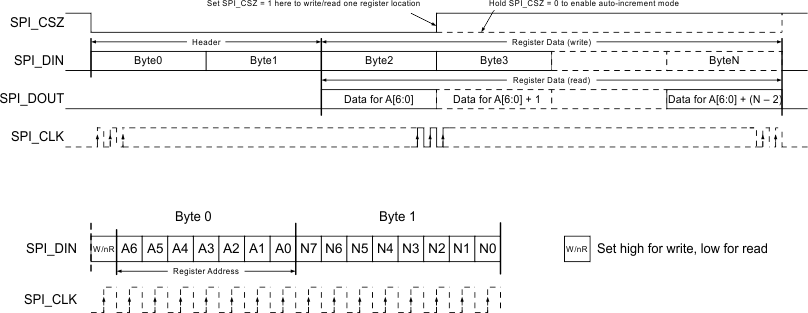
DLPA2000 provides a 4-wire SPI port that supports high-speed serial data transfers up to 33.3 MHz. Support includes register and data buffer write and read operations. The SPI_CSZ input serves as the active low chip select for the SPI port. The SPI_CSZ input must be forced low in order to write or read registers and data buffers. When SPI_CSZ is forced high, the data at the SPI_DIN input is ignored, and the SPI_DOUT output is forced to a high-impedance state. The SPI_DIN input serves as the serial data input for the port; the SPI_DOUT output serves as the serial data output. The SPI_CLK input serves as the serial data clock for both the input and output data. Data is latched at the SPI_DIN input on the rising edge of SPI_CLK, while data is clocked out of the SPI_DOUT output on the falling edge of SPI_CLK. Figure 13 shows the SPI port protocol. Byte 0 is referred to as the command byte, where the most significant bit is the write/not read bit. For the W/nR bit, a 1 indicates a write operation, while a 0 indicates a read operation. The remaining seven bits of the command byte are the register address targeted by the write or read operation. The SPI port supports write and read operations for multiple sequential register addresses through the implementation of an auto-increment mode. As shown in Figure 13, the auto-increment mode is invoked by simply holding the SPI_CSZ input low for multiple data bytes. The register address is automatically incremented after each data byte transferred, starting with the address specified by the command byte. After reaching address 0x7Fh the address pointer jumps back to 0x00h.
 Figure 13. SPI Protocol