ZHCSOK9A october 2021 – june 2023 DLPA300
PRODUCTION DATA
- 1
- 1 特性
- 2 应用
- 3 说明
- 4 Revision History
- 5 Pin Configuration and Functions
-
6 Specifications
- 6.1 Absolute Maximum Ratings
- 6.2 ESD Ratings
- 6.3 Recommended Operating Conditions
- 6.4 Thermal Information
- 6.5 Electrical Characteristics Control Logic
- 6.6 5-V Linear Regulator
- 6.7 Bias Voltage Boost Converter
- 6.8 Reset Voltage Buck-Boost Converter
- 6.9 VOFFSET Regulator
- 6.10 Switching Characteristics
- 7 Detailed Description
- 8 Application and Implementation
- 9 Power Supply Recommendations
- 10Layout
- 11Device and Documentation Support
- 12Mechanical, Packaging, and Orderable Information
6.10 Switching Characteristics
over operating free-air temperature range (unless otherwise noted)
| PARAMETER | TEST CONDITIONS | MIN | TYP | MAX | UNIT | |
|---|---|---|---|---|---|---|
| SERIAL COMMUNICATION PORT INTERFACE | ||||||
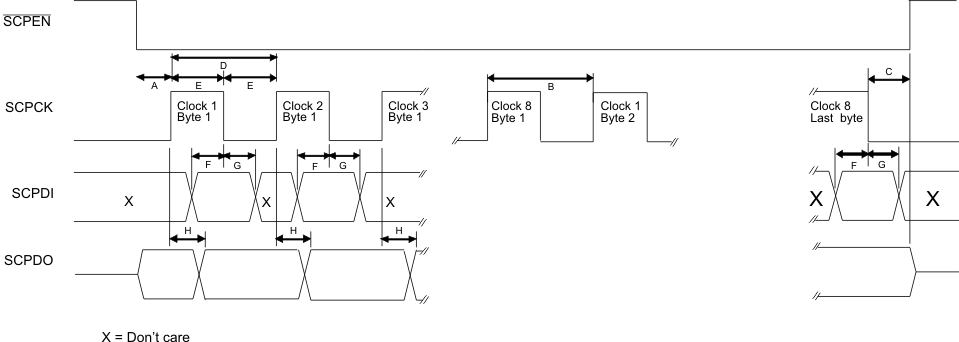
| A(1) | Setup SCPEN low to SCPCK | Reference to rising edge of SCPCK | 360 | ns | ||
| B(1) | Byte to byte delay | Nominally 1 SCPCK cycle, rising edge to rising edge | 1.9 | µs | ||
| C(1) | Setup SCPDI to SCPEN high | Last byte to secondary disable | 360 | ns | ||
| D(1) | SCPCK frequency(2) | 0 | 526 | kHz | ||
| SCPCK period | 1.9 | 2 | µs | |||
| E(1) | SCPCK high or low time | 300 | ns | |||
| F(1) | SCPDI set-up time | Reference to falling edge of SCPCK | 300 | ns | ||
| G(1) | SCPDI hold time | Reference from falling edge of SCPCK | 300 | ns | ||
| H(1) | SCPDO propagation delay | Reference from rising edge of SCPCK | 300 | ns | ||
| SCPEN, SCPCK, SCPDI, RESET filter (pulse reject) | 150 | ns | ||||
| OUTPUT MICROMIRROR CLOCKING PULSES | ||||||
| FPREP | Phased reset repetition frequency each output pin (non-overlapping) | 50 | kHz | |||
| FGREP | Global reset repetition frequency all output pins | 50 | kHz | |||
| IRLK | VRESET output leakage current | OE = 1, VRESET_RAIL = -28.5V | -1 | -10 | µA | |
| IBLK | VBIAS output leakage current | OE = 1, VBIAS_RAIL = 28.5V | 1 | 10 | µA | |
| IOLK | VOFFSET output leakage current | OE = 1, VOFFSET_RAIL = 10.25V | 1 | 10 | µA | |
| OUTPUT MICROMIRROR CLOCKING PULSE CONTROLS | ||||||
| tSPW | STROBE pulse width | 10 | ns | |||
| tSP | STROBE period | 20 | ns | |||
| tOHZ | Output time to high impedance | OE Pin = High | 100 | ns | ||
| tOEN | Output enable time from high impedance | OE Pin = Low | 100 | ns | ||
| tSUS | Set-up time | From A[3:0], MODE[1:0], and SEL[1:0] to STROBE edge | 8 | ns | ||
| tHOS | Hold time | From A[3:0], MODE[1:0], and SEL[1:0] to STROBE edge | 8 | ns | ||
| tPBR | Propagation time | From STROBE to VBIAS/VRESET edge 50% point. | 80 | 200 | ns | |
| tPRO | From STROBE to VRESET/VOFFSET edge 50% point. | 80 | 200 | ns | ||
| tPOB | From STROBE to VOFFSET/VBIAS edge 50% point. | 80 | 200 | ns | ||
| tDEL | Edge-to-edge propagation delta | Maximum difference between the slowest and fastest propagation times for any given reset output. | 40 | ns | ||
| tCHCH | Output channel-to-channel propagation delta | Maximum difference between the slowest and fastest propagation times for any two outputs for any given edge. | 20 | ns | ||
(1) See Figure 6-1
(2) There is no minimum speed for the serial port. It can be written to statically for diagnostic purposes.
 Figure 6-1 Serial Interface Timing