ZHCSIA7 May 2018 DLPA4000
PRODUCTION DATA.
- 1 特性
- 2 应用
- 3 说明
- 4 修订历史记录
- 5 Pin Configuration and Functions
- 6 Specifications
-
7 Detailed Description
- 7.1 Overview
- 7.2 Functional Block Description
- 7.3
Feature Description
- 7.3.1 Supply and Monitoring
- 7.3.2 Illumination
- 7.3.3 External Power MOSFET Selection
- 7.3.4 DMD Supplies
- 7.3.5 Buck Converters
- 7.3.6 Auxiliary LDOs
- 7.3.7 Measurement System
- 7.4 Device Functional Modes
- 7.5 Programming
- 7.6 Register Maps
- 8 Application and Implementation
- 9 Power Supply Recommendations
- 10Layout
- 11器件和文档支持
- 12机械、封装和可订购信息
7.3.2.4.3 Gate parallel capacitance (CG)
Use gate parallel capacitance specifically for higher supply voltages. The gate of a disabled power MOSFET can be pulled high parasitically due to a large drain voltage swing and the drain-gate capacitance,
In the low-side MOSFET this voltage swing can happen at the end of the non-overlap time while the power converter supplies current. In this case the switch node is low at the end of the non-overlap time. The switch node pulls high when the high-side MOSFET starts. Due to the large and steep waveform edge of the switch node current, the drain-gate capacitance of the low-side MOSFET injects the charge into the gate of the low-side FET. This situation causes the low-side MOSFET to operate for a short period of time causing a shoot-through current.
A similar situation exists with high-side FET. While the power converter discharges the LED voltage (VLED) the device directs the power converter current inward. At the end of the non-overlap time the switch node is high. If at that moment the low-side MOSFET is enabled, via the gate-drain capacitance of the high-side MOSFET charge is being injected into the gate of the high-side MOSFET potentially causing the device to switch on for a short amount of time. That switch-on behavior causes a shoot through current as well.
Add more gate-source filter capacitance to reduce the effect of the charge injection via the drain-source capacitance. In the case where a linear voltage division exists between gate-source capacitance and gate-drain capacitance, and for a 20-V supply voltage, maintain a ratio of gate-source capacitance and gate-drain capacitance to approximately 1:10 or larger. Make sure to test the gate-drive signals and the switch node for potential cross conduction.
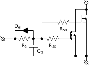
Sometimes a design can include dual MOSFETs to dissipate power (heat). Consider the configurations shown in Figure 7 tp prevent parasitic gate-oscillation a structure. In this example, the device isolates each gate with a resistor (RISO) to dampen potential oscillations. A resistance of 1 Ω is typically sufficient.
 Figure 7. Using RISO to Prevent Gate Oscillations When Using Power MOSFETs in Parallel
 A buck converter design requires at least two capacitors. Make sure that the value of the input-capacitor pin (ILLUM_A_VIN) is equal or greater than the selected output capacitance COUT, in this case ≥ 2 × 68 µF.