ZHCSIA7 May 2018 DLPA4000
PRODUCTION DATA.
- 1 特性
- 2 应用
- 3 说明
- 4 修订历史记录
- 5 Pin Configuration and Functions
- 6 Specifications
-
7 Detailed Description
- 7.1 Overview
- 7.2 Functional Block Description
- 7.3
Feature Description
- 7.3.1 Supply and Monitoring
- 7.3.2 Illumination
- 7.3.3 External Power MOSFET Selection
- 7.3.4 DMD Supplies
- 7.3.5 Buck Converters
- 7.3.6 Auxiliary LDOs
- 7.3.7 Measurement System
- 7.4 Device Functional Modes
- 7.5 Programming
- 7.6 Register Maps
- 8 Application and Implementation
- 9 Power Supply Recommendations
- 10Layout
- 11器件和文档支持
- 12机械、封装和可订购信息
9.1 Power-Up and Power-Down Timing
The power-up and power-down sequence ensures a correct operation of the DLPA4000 and to prevent damage to the DMD. The DLPA4000 controls the correct sequencing of the DMD_VRESET, DMD_VBIAS, and DMD_VOFFSET to ensure a reliable operation of the DMD.
The general startup sequence of the supplies is described earlier in Supply and Monitoring. The power-up sequence of the high voltage DMD lines is especially important in order not to damage the DMD. A too large delta voltage between DMD_VBIAS and DMD_VOFFSET could cause the damage and should therefore be prevented.
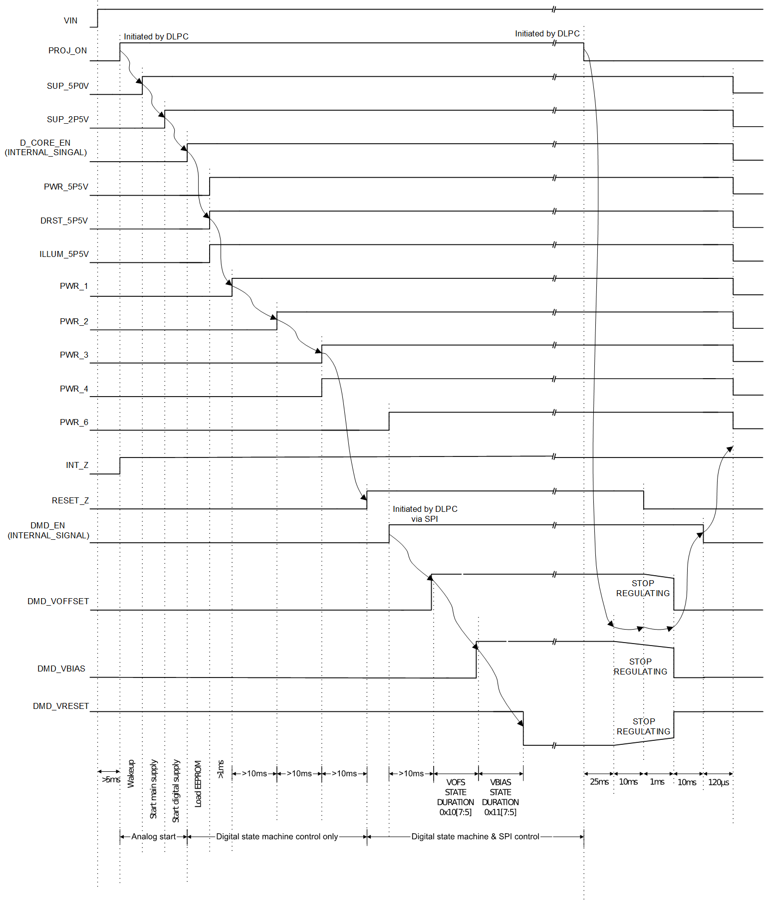
After the device pulls PROJ_ON high, the DMD buck converters and LDOs energize (PWR1, PWR2, PWR3, PWR4) the DMD high voltage lines (HV) sequentially enable. At the end of this sequence, the DLPA4000 becomes fully powered and ready for projection.
- DMD_VOFFSET
- delay
- VOFS_STATE_DURATION (register 0x10) DMD_VBIAS
- delay
- VBIAS_STATE_DURATION (register 0x11) DMD_VRESET
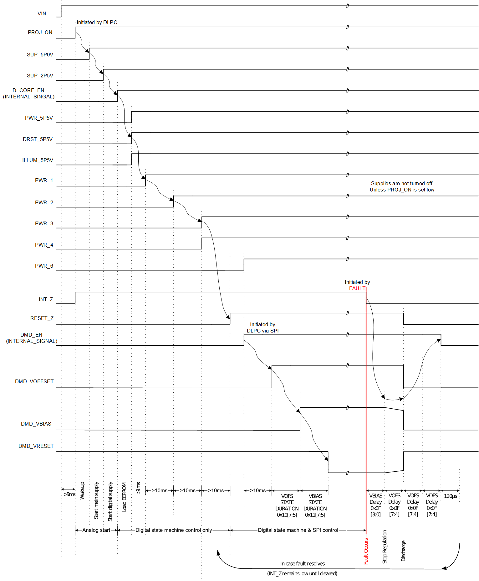
For shutdown there are two sequences, normal shutdown (Figure 23) and a fault fast shutdown used in case a fault occurs (Figure 24).
This is the shutdown sequence during normal mode operation
- 25-ms delay
- PROJ_ON pin goes low
- DMD_VBIAS and DMD_VRESET stop regulating
- 10 ms delay
- DMD_OFFSET stops regulating
- RESET_Z goes low
- 1 ms delay
- all three voltages discharge
- all other supplies de-energized
- INT_Z remains high
INT_Z remains high during the shutdown sequence because no fault occurred. During the power-down sequence the device makes sure the HV levels do not violate the DMD specifications on these three lines. For this it is important to select the capacitors such that CVOFFSET is equal to CVRESET and CVBIAS is ≤ CVOFFSET, CVBIAS.
The fast shutdown mode (Figure 24) sequence starts in case a fault occurs (INT_Z is pulled low), for instance due to overheating.
Use register 0x01 to enable and disable fast shutdown mode (FAST_SHUTDOWN_EN). Fast shutdown mode is the default mode. After the fault occurs, regulation of DMD_VBIAS and DMD_VRESET is stopped. The time (delay) between fault and stop of regulation can be controlled via register 0x0F (VBIAS/VRST_DELAY). The delay can be selected between 4 µs and approximately 1.1 ms, where the default is approximately 540 µs. A defined delay-time after the regulation stopped, all three high voltages lines are discharged and RESET_Z is pulled low. The delay can be controlled via register 0x0F (VOFS/VRESETZ_DELAY). Delay can be selected between 4 µs and approximately1.1ms. The default is ~4 µs. Finally the internal DMD_EN signal is pulled low.
The DLPA4000 device remains in standby state until the fault resolves. The device restarts then the fault resolves. The restart sequence begins when the device energizes the PWR_3 pin and follows the same steps as the regular startup sequence (see Figure 24). select capacitors so that CVOFFSET is equal to CVRESET and CVBIAS is ≤ CVOFFSET, CVBIAS. This selection criteria ensures proper discharge timing and discharge levels.

NOTE:
Arrows indicate sequence of events automatically controlled by digital state machine. Other events are initiated under SPI control.
NOTE:
Arrows indicate sequence of events automatically controlled by digital state machine. Other events are initiated under SPI control.