ZHCSIA7 May 2018 DLPA4000
PRODUCTION DATA.
- 1 特性
- 2 应用
- 3 说明
- 4 修订历史记录
- 5 Pin Configuration and Functions
- 6 Specifications
-
7 Detailed Description
- 7.1 Overview
- 7.2 Functional Block Description
- 7.3
Feature Description
- 7.3.1 Supply and Monitoring
- 7.3.2 Illumination
- 7.3.3 External Power MOSFET Selection
- 7.3.4 DMD Supplies
- 7.3.5 Buck Converters
- 7.3.6 Auxiliary LDOs
- 7.3.7 Measurement System
- 7.4 Device Functional Modes
- 7.5 Programming
- 7.6 Register Maps
- 8 Application and Implementation
- 9 Power Supply Recommendations
- 10Layout
- 11器件和文档支持
- 12机械、封装和可订购信息
10.1.5 LED Connection
Large switched currents flow through the wiring from the external RGB switches to the LEDs. Consider these two specifications to optimize the LED-to-RGB switches wiring layout:
- wiring resistancce, RSERIES
- wiring inductance, LSERIES
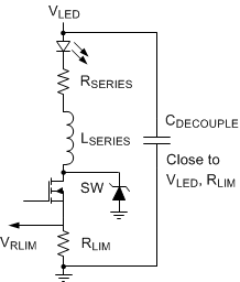
Figure 32 shows the parasitic series impedances.
 Figure 32. Parasitic Inductance (LSeries) and Resistance (Rseries) in Series with LED
 Currents up to 32 A can flow through the wires connecting the LEDs to the RGB switches. The layout can cause noticeable dissipation. Every 10 mΩ of series resistances implies a parasitic power dissipation of 5 W for a 32 A (avg) LED current . This dissipation can cause an increase in PCB temperature, and more importantly, deterioration of overall system efficiency.
The wiring resistance may impact the control dynamics of the LED current. The LED current control loop includes the routing resistance. The LED voltage (VLED) controlls the LED current. Use Equation 15 to calculate the total differential resistance of a path RSERIES.
where
- ΔILED is the LED current variation
- ΔVLED is a small change in VLED
- rLED is the differential resistance of the LED
- Ron_SW_P,Q,R the on-resistance of the strobe decoder switch
- LSERIES is ignored

Equation 15 ignores LSERIES because realistic values are usually sufficiently low to cause any noticeable impact on the dynamics
All differential resistance values range from about 4 mΩ to several hundreds of mΩ. Applications can yield a series resistance of 100 mΩ if the layout guidelines are not followed. Make sure the application series resistance is <10 mΩ.
The series inductance plays an important role when considering the switched nature of the LED current. the current switches through R,G and B LEDs quickly. The turn-off time is significantly fast. A current of 32 A goes to 0 A in 50 ns. This speed causes a voltage spike of approximately 1 V for every 5 nH of parasitic inductance. Minimize the series inductance of the LED wiring by designing an application that has these features:
- Short wires
- Thick wires or multiple parallel wires
- Small enclosed area of the forward and return current path
Use a diode when the application cannot be designed to yield a sufficiently low inductance. Use a Zener diode to clamp the drain voltage of the RGB switch so that it remains below the absolute maximum rating. Choose a clamping voltage between the maximum expected VLED and the absolute maximum rating. Make sure the clamping voltage has sufficient margin relative to the minimum and maximum voltage.