ZHCSIA7 May 2018 DLPA4000
PRODUCTION DATA.
- 1 特性
- 2 应用
- 3 说明
- 4 修订历史记录
- 5 Pin Configuration and Functions
- 6 Specifications
-
7 Detailed Description
- 7.1 Overview
- 7.2 Functional Block Description
- 7.3
Feature Description
- 7.3.1 Supply and Monitoring
- 7.3.2 Illumination
- 7.3.3 External Power MOSFET Selection
- 7.3.4 DMD Supplies
- 7.3.5 Buck Converters
- 7.3.6 Auxiliary LDOs
- 7.3.7 Measurement System
- 7.4 Device Functional Modes
- 7.5 Programming
- 7.6 Register Maps
- 8 Application and Implementation
- 9 Power Supply Recommendations
- 10Layout
- 11器件和文档支持
- 12机械、封装和可订购信息
10.2 Layout Example
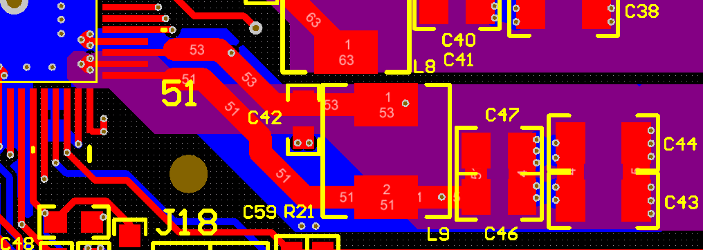
Figure 33 shows an example of a proper buck converter layout. It shows the routing and placing of the components near the DLPA4000 for optimal performance. A register sets the output voltage of the converters used by the DLPA4000. The DLPA4000 uses the feedback pin to compare the output voltage with an internal setpoint.
 Figure 33. Practical Layout Example
 Use short traces. Separate individual power grounds to avoid ground shift problems. Ground shift problems occur when ground currents of different buck converters interfere. High currents flow through the inductor (L7) and the output capacitors (C130, C131).Make the traces to and from inductor and capacitors as short as possible to avoid losses due to trace resistance. Use high-quality capacitors with a low ESR value to minimize losses in the capacitors and to maintain an acceptable amount of voltage ripple.
In order to prevent problems with switching high currents at high frequencies the layout is very critical and snubber networks are advisable. The switching frequency can vary from several hundreds of kHz to frequencies in the MHz range. Keep in mind that it takes only nanoseconds to switch currents from zero to several amperes which is equivalent to even much higher frequencies. Those switching moments causes EMI problems if not properly handled, especially when ringing occurs on the edges, which can have higher amplitude and frequency as the switching voltage itself. To prevent this ringing the DLPA4000 buck converters all need a snubber network, consisting of a resistor and a capacitor in series implemented on the board to reduce this unwanted behavior. The snubber network is in this case placed on the bottom-side of the PCB (thus not visible here) connected to the trace of L9 routing to the switch node.
In order to make more clear what plays a role when laying out a buck converter, this paragraph explains the connections and placing of the parts around the buck converter connected to the pins 50-54. The supply voltage is connected to pin 52 which is laid out on a mid layer (purple colored) and is connected to this pin using 3 via’s to make sure a stable and low resistance connection is made. The decoupling is done by capacitor C43 & C44 visible on the bottom right of Figure 33 and the connection to the supply and the ground layer is done using multiple vias. The ground connection on pin 54 is also done using multiple vias to the ground layer which is visible as the blue areas in Figure 33. By using different layers it is possible to create low resistive paths. Ideally the ground connection of the output capacitors and the ground connection of the part (pin54) should be close together. The layout connects both points together using a wide trace on the bottom layer (blue colored area) which is also suitable to bring both connections together. All buck converters in the layout have the same layout structure and use a separated ground trace to their respective ground connection on the part. All these ground connections are connected together on the ground plane below the DLPA4000 itself. shows the position of the converter inductor and its accompanying capacitors (L9 & C46, C47) as close as possible positioned to the pins 51 and 53 using traces as thick as possible. The ground connections of these capacitors is done using multiple via’s to the ground layer to ensure a low resistance path.