ZHCSDJ3C March 2015 – June 2019 DLPC150
PRODUCTION DATA.
- 1 特性
- 2 应用
- 3 说明
- 4 修订历史记录
- 5 Pin Configuration and Functions
-
6 Specifications
- 6.1 Absolute Maximum Ratings
- 6.2 ESD Ratings
- 6.3 Recommended Operating Conditions
- 6.4 Thermal Information
- 6.5 Electrical Characteristics Over Recommended Operating Conditions
- 6.6 Electrical Characteristics
- 6.7 High-Speed Sub-LVDS Electrical Characteristics
- 6.8 Low-Speed SDR Electrical Characteristics
- 6.9 System Oscillators Timing Requirements
- 6.10 Power-Up and Reset Timing Requirements
- 6.11 Parallel Interface Frame Timing Requirements
- 6.12 Parallel Interface General Timing Requirements
- 6.13 Flash Interface Timing Requirements
- 7 Parameter Measurement Information
- 8 Detailed Description
- 9 Application and Implementation
- 10Power Supply Recommendations
-
11Layout
- 11.1
Layout Guidelines
- 11.1.1 PCB Layout Guidelines For Internal Controller PLL Power
- 11.1.2 DLPC150 Reference Clock
- 11.1.3 General PCB Recommendations
- 11.1.4 General Handling Guidelines for Unused CMOS-Type Pins
- 11.1.5 Maximum Pin-to-Pin, PCB Interconnects Etch Lengths
- 11.1.6 Number of Layer Changes
- 11.1.7 Stubs
- 11.1.8 Terminations
- 11.1.9 Routing Vias
- 11.2 Layout Example
- 11.3 Thermal Considerations
- 11.1
Layout Guidelines
- 12器件和文档支持
- 13"机械、封装和可订购信息
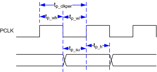
6.12 Parallel Interface General Timing Requirements(2)
| MIN | MAX | UNIT | |||
|---|---|---|---|---|---|
| ƒclock | Clock frequency, PCLK | 1 | 75 | MHz | |
| tp_clkper | Clock period, PCLK | 50% reference points | 6.66 | 1000 | ns |
| tp_clkjit | Clock jitter, PCLK | Max ƒclock | see (1) | see (1) | |
| tp_wh | Pulse duration low, PCLK | 50% reference points | 2.43 | ns | |
| tp_wl | Pulse duration high, PCLK | 50% reference points | 2.43 | ns | |
| tp_su | Setup time – HSYNC_CS, DATEN_CMD, PDATA(23:0) valid before the active edge of PCLK | 50% reference points | 0.9 | ns | |
| tp_h | Hold time – HSYNC_CS, DATEN_CMD, PDATA(23:0) valid after the active edge of PCLK | 50% reference points | 0.9 | ns | |
| tt | Transition time – all signals | 20% to 80% reference points | 0.2 | 2 | ns |
(1) Clock jitter (in ns) should be calculated using this formula: Jitter = [1 / ƒclock – 5.76 ns]. Setup and hold times must be met during clock jitter.
(2) The active (capture) edge of PCLK for HSYNC_CS, DATEN_CMD and PDATA(23:0) is software programmable, but defaults to the rising edge.
 Figure 6. Parallel Interface General Timing