ZHCSDJ3C March 2015 – June 2019 DLPC150
PRODUCTION DATA.
- 1 特性
- 2 应用
- 3 说明
- 4 修订历史记录
- 5 Pin Configuration and Functions
-
6 Specifications
- 6.1 Absolute Maximum Ratings
- 6.2 ESD Ratings
- 6.3 Recommended Operating Conditions
- 6.4 Thermal Information
- 6.5 Electrical Characteristics Over Recommended Operating Conditions
- 6.6 Electrical Characteristics
- 6.7 High-Speed Sub-LVDS Electrical Characteristics
- 6.8 Low-Speed SDR Electrical Characteristics
- 6.9 System Oscillators Timing Requirements
- 6.10 Power-Up and Reset Timing Requirements
- 6.11 Parallel Interface Frame Timing Requirements
- 6.12 Parallel Interface General Timing Requirements
- 6.13 Flash Interface Timing Requirements
- 7 Parameter Measurement Information
- 8 Detailed Description
- 9 Application and Implementation
- 10Power Supply Recommendations
-
11Layout
- 11.1
Layout Guidelines
- 11.1.1 PCB Layout Guidelines For Internal Controller PLL Power
- 11.1.2 DLPC150 Reference Clock
- 11.1.3 General PCB Recommendations
- 11.1.4 General Handling Guidelines for Unused CMOS-Type Pins
- 11.1.5 Maximum Pin-to-Pin, PCB Interconnects Etch Lengths
- 11.1.6 Number of Layer Changes
- 11.1.7 Stubs
- 11.1.8 Terminations
- 11.1.9 Routing Vias
- 11.2 Layout Example
- 11.3 Thermal Considerations
- 11.1
Layout Guidelines
- 12器件和文档支持
- 13"机械、封装和可订购信息
11.1.1 PCB Layout Guidelines For Internal Controller PLL Power
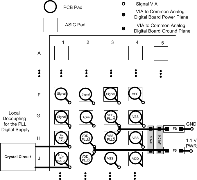
The following guidelines are recommended to achieve desired controller performance relative to the internal PLL. The DLPC150 contains 2 internal PLLs which have dedicated analog supplies (VDD_PLLM , VSS_PLLM, VDD_PLLD, VSS_PLLD). As a minimum, VDD_PLLx power and VSS_PLLx ground pins should be isolated using a simple passive filter consisting of two series Ferrites and two shunt capacitors (to widen the spectrum of noise absorption). It’s recommended that one capacitor be a 0.1µF capacitor and the other be a 0.01µF capacitor. All four components should be placed as close to the controller as possible but it’s especially important to keep the leads of the high frequency capacitors as short as possible. Note that both capacitors should be connected across VDD_PLLM and VSS_PLLM / VDD_PLLD and VSS_PLLD respectfully on the controller side of the Ferrites.
For the ferrite beads used, their respective characteristics should be as follows:
- DC resistance less than 0.40 Ω
- Impedance at 10 MHz equal to or greater than 180 Ω
- Impedance at 100 MHz equal to or greater than 600 Ω
The PCB layout is critical to PLL performance. It is vital that the quiet ground and power are treated like analog signals. Therefore, VDD_PLLM and VDD_PLLD must be a single trace from the DLPC150 to both capacitors and then through the series ferrites to the power source. The power and ground traces should be as short as possible, parallel to each other, and as close as possible to each other.
 Figure 17. PLL Filter Layout