ZHCSLG8E August 2020 – August 2024 DLPC230S-Q1 , DLPC231S-Q1
PRODUCTION DATA
- 1
- 1 特性
- 2 应用
- 3 说明
- 4 Pin Configuration and Functions
-
5 Specifications
- 5.1 Absolute Maximum Ratings
- 5.2 ESD Ratings
- 5.3 Recommended Operating Conditions
- 5.4 Thermal Information
- 5.5 Electrical Characteristics
- 5.6 Electrical Characteristics for Fixed Voltage I/O
- 5.7 DMD High-Speed SubLVDS Electrical Characteristics
- 5.8 DMD Low-Speed SubLVDS Electrical Characteristics
- 5.9 OpenLDI LVDS Electrical Characteristics
- 5.10 Power Dissipation Characterisics
- 5.11 System Oscillators Timing Requirements
- 5.12 Power Supply and Reset Timing Requirements
- 5.13 Parallel Interface General Timing Requirements
- 5.14 OpenLDI Interface General Timing Requirements
- 5.15 Parallel/OpenLDI Interface Frame Timing Requirements
- 5.16 Host/Diagnostic Port SPI Interface Timing Requirements
- 5.17 Host/Diagnostic Port I2C Interface Timing Requirements
- 5.18 Flash Interface Timing Requirements
- 5.19 TPS99000S-Q1 SPI Interface Timing Requirements
- 5.20 TPS99000S-Q1 AD3 Interface Timing Requirements
- 5.21 DLPC23xS-Q1 I2C Port Interface Timing Requirements
- 5.22 Chipset Component Usage Specification
- 6 Parameter Measurement Information
-
7 Detailed Description
- 7.1 Overview
- 7.2 Functional Block Diagram
- 7.3
Feature Description
- 7.3.1 Parallel Interface
- 7.3.2 OpenLDI Interface
- 7.3.3 DMD (SubLVDS) Interface
- 7.3.4 Serial Flash Interface
- 7.3.5 Serial Flash Programming
- 7.3.6 Host Command and Diagnostic Processor Interfaces
- 7.3.7 GPIO Supported Functionality
- 7.3.8 Built-In Self Test (BIST)
- 7.3.9 EEPROMs
- 7.3.10 Temperature Sensor
- 7.3.11 Debug Support
- 7.4 Device Functional Modes
-
8 Application and Implementation
- 8.1 Application Information
- 8.2 Typical Application
- 8.3 Power Supply Recommendations
- 8.4
Layout
- 8.4.1
Layout Guidelines
- 8.4.1.1 PCB Layout Guidelines for Internal ASIC PLL Power
- 8.4.1.2 DLPC23xS-Q1 Reference Clock
- 8.4.1.3 DMD Interface Layout Considerations
- 8.4.1.4 General PCB Recommendations
- 8.4.1.5 General Handling Guidelines for Unused CMOS-Type Pins
- 8.4.1.6 Maximum Pin-to-Pin, PCB Interconnects Etch Lengths
- 8.4.1.7 Number of Layer Changes
- 8.4.1.8 Stubs
- 8.4.1.9 Terminations
- 8.4.1.10 Routing Vias
- 8.4.2 Thermal Considerations
- 8.4.1
Layout Guidelines
- 9 Device and Documentation Support
- 10Revision History
- 11Mechanical, Packaging, and Orderable Information
8.4.1.2.1 Recommended Crystal Oscillator Configuration
Table 8-2 Recommended Crystal Configuration
| PARAMETER | RECOMMENDED | UNIT |
|---|---|---|
| Crystal circuit configuration | Parallel resonant | |
| Crystal type | Fundamental (first harmonic) | |
| Crystal nominal frequency | 16 | MHz |
| Crystal frequency tolerance (including accuracy, temperature, aging and trim sensitivity) | ±200 | PPM |
| Maximum crystal equivalent series resistance (ESR) | 50 | Ω |
| Crystal load capacitance | 10 | pF |
| Temperature range | –40°C to +105°C | °C |
| Drive level (nominal) | 100 | µW |
| RFB feedback resistor (nominal) | 1 | MΩ |
| CL1 external crystal load capacitor | See equation in (1) | pF |
| CL2 external crystal load capacitor | See equation in (2) | pF |
| PCB layout | A ground isolation ring around the crystal is recommended |
(1) CL1 = 2 × (CL – Cstray_pll_refclk_i), where: Cstray_pll_refclk_i = Sum of the package and PCB stray capacitance at the crystal pin associated with the ASIC pin pll_refclk_i.
(2) CL2 = 2 × (CL – Cstray_pll_refclk_o), where: Cstray_pll_refclk_o = Sum of the package and PCB stray capacitance at the crystal pin associated with the ASIC pin pll_refclk_o.
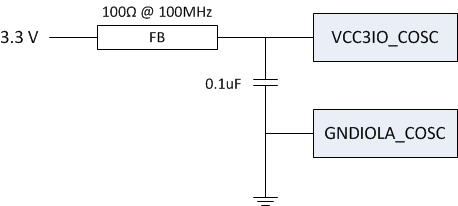
The crystal circuit in the DLPC23xS-Q1 ASIC has dedicated power (VCC3IO_COSC) and ground (GNDIOLA_COSC) pins, with the recommended filtering shown in Figure 8-13.
 Figure 8-13 Crystal Power Supply Filtering
Table 8-3 DLPC23xS-Q1 Recommended Crystal Parts
| MANUFACTURER | PART NUMBER | SPEED | FREQUENCY TOLERANCE, FREQUENCY STABILITY, AGING/YEAR | ESR | LOAD CAPACITANCE | OPERATING TEMPERATURE |
|---|---|---|---|---|---|---|
| TXC | AM16070006(1) | 16MHz | Freq Tolerance: ±10ppm | 50Ω max | 10pF | –40°C to +125°C |
| Freq Stability: ±50ppm | ||||||
| Aging/Year: ±3ppm |
(1) This device requires a 3kΩ series resister to limit power.
If an external oscillator is used, the oscillator output must drive the PLL_REFCLK_O pin on the DLPC23xS-Q1 ASIC, the PLL_REFCLK_I pin must be left unconnected, and the OSC_BYPASS pin must = logic HIGH.