ZHCSLG8E August 2020 – August 2024 DLPC230S-Q1 , DLPC231S-Q1
PRODUCTION DATA
- 1
- 1 特性
- 2 应用
- 3 说明
- 4 Pin Configuration and Functions
-
5 Specifications
- 5.1 Absolute Maximum Ratings
- 5.2 ESD Ratings
- 5.3 Recommended Operating Conditions
- 5.4 Thermal Information
- 5.5 Electrical Characteristics
- 5.6 Electrical Characteristics for Fixed Voltage I/O
- 5.7 DMD High-Speed SubLVDS Electrical Characteristics
- 5.8 DMD Low-Speed SubLVDS Electrical Characteristics
- 5.9 OpenLDI LVDS Electrical Characteristics
- 5.10 Power Dissipation Characterisics
- 5.11 System Oscillators Timing Requirements
- 5.12 Power Supply and Reset Timing Requirements
- 5.13 Parallel Interface General Timing Requirements
- 5.14 OpenLDI Interface General Timing Requirements
- 5.15 Parallel/OpenLDI Interface Frame Timing Requirements
- 5.16 Host/Diagnostic Port SPI Interface Timing Requirements
- 5.17 Host/Diagnostic Port I2C Interface Timing Requirements
- 5.18 Flash Interface Timing Requirements
- 5.19 TPS99000S-Q1 SPI Interface Timing Requirements
- 5.20 TPS99000S-Q1 AD3 Interface Timing Requirements
- 5.21 DLPC23xS-Q1 I2C Port Interface Timing Requirements
- 5.22 Chipset Component Usage Specification
- 6 Parameter Measurement Information
-
7 Detailed Description
- 7.1 Overview
- 7.2 Functional Block Diagram
- 7.3
Feature Description
- 7.3.1 Parallel Interface
- 7.3.2 OpenLDI Interface
- 7.3.3 DMD (SubLVDS) Interface
- 7.3.4 Serial Flash Interface
- 7.3.5 Serial Flash Programming
- 7.3.6 Host Command and Diagnostic Processor Interfaces
- 7.3.7 GPIO Supported Functionality
- 7.3.8 Built-In Self Test (BIST)
- 7.3.9 EEPROMs
- 7.3.10 Temperature Sensor
- 7.3.11 Debug Support
- 7.4 Device Functional Modes
-
8 Application and Implementation
- 8.1 Application Information
- 8.2 Typical Application
- 8.3 Power Supply Recommendations
- 8.4
Layout
- 8.4.1
Layout Guidelines
- 8.4.1.1 PCB Layout Guidelines for Internal ASIC PLL Power
- 8.4.1.2 DLPC23xS-Q1 Reference Clock
- 8.4.1.3 DMD Interface Layout Considerations
- 8.4.1.4 General PCB Recommendations
- 8.4.1.5 General Handling Guidelines for Unused CMOS-Type Pins
- 8.4.1.6 Maximum Pin-to-Pin, PCB Interconnects Etch Lengths
- 8.4.1.7 Number of Layer Changes
- 8.4.1.8 Stubs
- 8.4.1.9 Terminations
- 8.4.1.10 Routing Vias
- 8.4.2 Thermal Considerations
- 8.4.1
Layout Guidelines
- 9 Device and Documentation Support
- 10Revision History
- 11Mechanical, Packaging, and Orderable Information
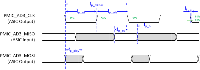
5.20 TPS99000S-Q1 AD3 Interface Timing Requirements
The DLPC23xS-Q1 ASIC to TPS99000S-Q1 AD3 interface is used to retrieve ADC
measurements from the TPS99000S-Q1. The interface is similar to SPI and includes a
clock, MOSI, and MISO signal.
| (1)(2)(3) | MIN | MAX | UNIT | ||
|---|---|---|---|---|---|
| fclock | Clock frequency, PMIC_AD3_CLK | 29.326 | 30.006 | MHz | |
| tp_clkper | Clock period, PMIC_AD3_CLK (50% reference points) | 33.327 | 34.100 | ns | |
| tp_wh | Pulse duration high, PMIC_AD3_CLK (50% reference points) (Referenced to tp_clkper) | 40% | |||
| tp_wl | Pulse duration low, PMIC_AD3_CLK (50% reference points) (Referenced to tp_clkper) | 40% | |||
| tt | Transition time – all input signals | 20% to 80% reference points | 6 | ns | |
| tp_su | Setup time –
PMIC_AD3_MISO valid before PMIC_AD3_CLK falling edge (50% reference points) | 14.5 | ns | ||
| tp_h | Hold time –
PMIC_AD3_MISO valid after PMIC_AD3_CLK falling edge (50% reference points) | 0 | ns | ||
| tp_clqv | PMIC_AD3_MOSI
output delay (valid) time (with respect to falling edge of
PMIC_AD3_CLK) (50% reference points) | –2.0 | 2.0 | ns | |
(1) PMIC_AD3_MOSI ((DLPC23xS-Q1) Output / (TPS99000S-Q1) Input) is transmitted on the
falling edge of PMIC_AD3_CLK.
(2) PMIC_AD3_MISO ((DLPC23xS-Q1) Input / (TPS99000S-Q1) Output) is captured on the
rising edge of PMIC_AD3_CLK.
(3) PMIC_AD3_CLK is used as the primary TPS99000S-Q1 system clock in addition to supporting the AD3 interface.
 Figure 5-11 TPS99000S-Q1 AD3 Interface Timing
 Figure 5-12 TPS99000S-Q1 AD3 Data Capture and Transition