ZHCSLG8E August 2020 – August 2024 DLPC230S-Q1 , DLPC231S-Q1
PRODUCTION DATA
- 1
- 1 特性
- 2 应用
- 3 说明
- 4 Pin Configuration and Functions
-
5 Specifications
- 5.1 Absolute Maximum Ratings
- 5.2 ESD Ratings
- 5.3 Recommended Operating Conditions
- 5.4 Thermal Information
- 5.5 Electrical Characteristics
- 5.6 Electrical Characteristics for Fixed Voltage I/O
- 5.7 DMD High-Speed SubLVDS Electrical Characteristics
- 5.8 DMD Low-Speed SubLVDS Electrical Characteristics
- 5.9 OpenLDI LVDS Electrical Characteristics
- 5.10 Power Dissipation Characterisics
- 5.11 System Oscillators Timing Requirements
- 5.12 Power Supply and Reset Timing Requirements
- 5.13 Parallel Interface General Timing Requirements
- 5.14 OpenLDI Interface General Timing Requirements
- 5.15 Parallel/OpenLDI Interface Frame Timing Requirements
- 5.16 Host/Diagnostic Port SPI Interface Timing Requirements
- 5.17 Host/Diagnostic Port I2C Interface Timing Requirements
- 5.18 Flash Interface Timing Requirements
- 5.19 TPS99000S-Q1 SPI Interface Timing Requirements
- 5.20 TPS99000S-Q1 AD3 Interface Timing Requirements
- 5.21 DLPC23xS-Q1 I2C Port Interface Timing Requirements
- 5.22 Chipset Component Usage Specification
- 6 Parameter Measurement Information
-
7 Detailed Description
- 7.1 Overview
- 7.2 Functional Block Diagram
- 7.3
Feature Description
- 7.3.1 Parallel Interface
- 7.3.2 OpenLDI Interface
- 7.3.3 DMD (SubLVDS) Interface
- 7.3.4 Serial Flash Interface
- 7.3.5 Serial Flash Programming
- 7.3.6 Host Command and Diagnostic Processor Interfaces
- 7.3.7 GPIO Supported Functionality
- 7.3.8 Built-In Self Test (BIST)
- 7.3.9 EEPROMs
- 7.3.10 Temperature Sensor
- 7.3.11 Debug Support
- 7.4 Device Functional Modes
-
8 Application and Implementation
- 8.1 Application Information
- 8.2 Typical Application
- 8.3 Power Supply Recommendations
- 8.4
Layout
- 8.4.1
Layout Guidelines
- 8.4.1.1 PCB Layout Guidelines for Internal ASIC PLL Power
- 8.4.1.2 DLPC23xS-Q1 Reference Clock
- 8.4.1.3 DMD Interface Layout Considerations
- 8.4.1.4 General PCB Recommendations
- 8.4.1.5 General Handling Guidelines for Unused CMOS-Type Pins
- 8.4.1.6 Maximum Pin-to-Pin, PCB Interconnects Etch Lengths
- 8.4.1.7 Number of Layer Changes
- 8.4.1.8 Stubs
- 8.4.1.9 Terminations
- 8.4.1.10 Routing Vias
- 8.4.2 Thermal Considerations
- 8.4.1
Layout Guidelines
- 9 Device and Documentation Support
- 10Revision History
- 11Mechanical, Packaging, and Orderable Information
8.4.1.1 PCB Layout Guidelines for Internal ASIC PLL Power
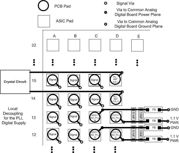
The following guidelines are recommended to achieve the desired ASIC performance relative to the internal PLL. The DLPC23xS-Q1 contains two internal PLLs that have dedicated analog supplies (VCC11AD_PLLM, GND11AD_PLLM, VCC11AD_PLLD, GND11AD_PLLD). At a minimum, VCC11AD_PLLx power and GND11AD_PLLx ground pins must be isolated using a simple passive filter consisting of two series ferrites and two shunt capacitors (to widen the spectrum of noise absorption). Recommended values and layout are shown in Table 8-1 and Figure 8-10, respectively.
| COMPONENT | PARAMETER | RECOMMENDED VALUE | UNIT |
|---|---|---|---|
| Shunt Capacitor | Capacitance | 0.1 | µF |
| Shunt Capacitor | Capacitance | 1.0 | µF |
| Series Ferrite | Impedance at 100 MHz | > 100 | Ω |
| DC Resistance | < 0.40 |
Because the PCB layout is critical to PLL performance, it is vital that the quiet ground and power are treated like analog signals. Additional design guidelines are as follows:
- All four components must be placed as close to the ASIC as possible.
- It is especially important to keep the leads of the high-frequency capacitors as short as possible.
- A capacitor of each value must be connected across VCC11AD_PLLM / GND11AD_PLLM and VCC11AD_PLLD / GND11AD_PLLD respectively on the ASIC side of the ferrites.
- VCC11AD_PLLM and VCC11AD_PLLD must be a single trace from the DLPC23xS-Q1 to both capacitors and then through the series of ferrites to the power source.
- The power and ground traces must be as short as possible, parallel to each other, and as close as possible to each other.
 Figure 8-10 DLPC230S-Q1 PLL Filter Layout
 Figure 8-11 DLPC231S-Q1 PLL Filter and Crystal Layout