ZHCSLG8E August 2020 – August 2024 DLPC230S-Q1 , DLPC231S-Q1
PRODUCTION DATA
- 1
- 1 特性
- 2 应用
- 3 说明
- 4 Pin Configuration and Functions
-
5 Specifications
- 5.1 Absolute Maximum Ratings
- 5.2 ESD Ratings
- 5.3 Recommended Operating Conditions
- 5.4 Thermal Information
- 5.5 Electrical Characteristics
- 5.6 Electrical Characteristics for Fixed Voltage I/O
- 5.7 DMD High-Speed SubLVDS Electrical Characteristics
- 5.8 DMD Low-Speed SubLVDS Electrical Characteristics
- 5.9 OpenLDI LVDS Electrical Characteristics
- 5.10 Power Dissipation Characterisics
- 5.11 System Oscillators Timing Requirements
- 5.12 Power Supply and Reset Timing Requirements
- 5.13 Parallel Interface General Timing Requirements
- 5.14 OpenLDI Interface General Timing Requirements
- 5.15 Parallel/OpenLDI Interface Frame Timing Requirements
- 5.16 Host/Diagnostic Port SPI Interface Timing Requirements
- 5.17 Host/Diagnostic Port I2C Interface Timing Requirements
- 5.18 Flash Interface Timing Requirements
- 5.19 TPS99000S-Q1 SPI Interface Timing Requirements
- 5.20 TPS99000S-Q1 AD3 Interface Timing Requirements
- 5.21 DLPC23xS-Q1 I2C Port Interface Timing Requirements
- 5.22 Chipset Component Usage Specification
- 6 Parameter Measurement Information
-
7 Detailed Description
- 7.1 Overview
- 7.2 Functional Block Diagram
- 7.3
Feature Description
- 7.3.1 Parallel Interface
- 7.3.2 OpenLDI Interface
- 7.3.3 DMD (SubLVDS) Interface
- 7.3.4 Serial Flash Interface
- 7.3.5 Serial Flash Programming
- 7.3.6 Host Command and Diagnostic Processor Interfaces
- 7.3.7 GPIO Supported Functionality
- 7.3.8 Built-In Self Test (BIST)
- 7.3.9 EEPROMs
- 7.3.10 Temperature Sensor
- 7.3.11 Debug Support
- 7.4 Device Functional Modes
-
8 Application and Implementation
- 8.1 Application Information
- 8.2 Typical Application
- 8.3 Power Supply Recommendations
- 8.4
Layout
- 8.4.1
Layout Guidelines
- 8.4.1.1 PCB Layout Guidelines for Internal ASIC PLL Power
- 8.4.1.2 DLPC23xS-Q1 Reference Clock
- 8.4.1.3 DMD Interface Layout Considerations
- 8.4.1.4 General PCB Recommendations
- 8.4.1.5 General Handling Guidelines for Unused CMOS-Type Pins
- 8.4.1.6 Maximum Pin-to-Pin, PCB Interconnects Etch Lengths
- 8.4.1.7 Number of Layer Changes
- 8.4.1.8 Stubs
- 8.4.1.9 Terminations
- 8.4.1.10 Routing Vias
- 8.4.2 Thermal Considerations
- 8.4.1
Layout Guidelines
- 9 Device and Documentation Support
- 10Revision History
- 11Mechanical, Packaging, and Orderable Information
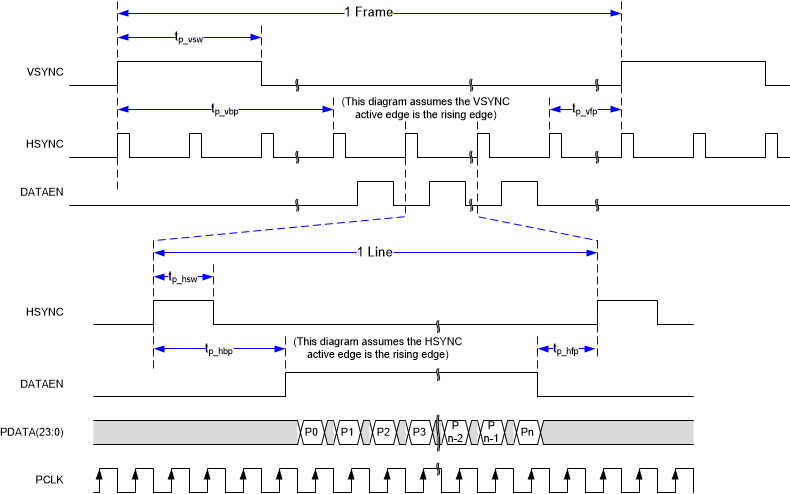
5.15 Parallel/OpenLDI Interface Frame Timing Requirements
See(1)
| MIN | MAX | UNIT | |||
|---|---|---|---|---|---|
| VSYNC | Vertical Sync Rate (for the specified active source resolution) | See Section 6.2.1 for supported resolutions. | 58 | 61 | Hz |
| tp_vsw | Pulse duration – VSYNC high | 50% reference points | 1 | lines | |
| tp_vbp | Vertical back porch (VBP) – time from the leading edge of VSYNC to the leading edge HSYNC for the first active line (includes tp_vsw). | 50% reference points | 2 | lines | |
| tp_vƒp | Vertical front porch (VFP) – time from the leading edge of the HSYNC following the last active line in a frame to the leading edge of VSYNC | 50% reference points | 1 | lines | |
| tp_tvb | Total vertical blanking – time from the leading edge of HSYNC following the last active line of one frame to the leading edge of HSYNC for the first active line in the next frame. (This is equal to the sum of VBP (tp_vbp) + VFP (tp_vfp)) | 50% reference points | 14 | lines | |
| tp_hsw | Pulse duration – HSYNC high | 50% reference points | 8 | PCLKs | |
| tp_hbp | Horizontal back porch – time from rising edge of HSYNC to rising edge of DATEN (includes tp_hsw) | 50% reference points | 9 | PCLKs | |
| tp_hfp | Horizontal front porch – time from falling edge of DATEN to rising edge of HSYNC | 50% reference points | 8 | PCLKs | |
| tp_thb | Total horizontal blanking | 50% reference points | 64 | PCLKs | |
| TPPL | Total Pixels Per Line | 8191 | Pixels | ||
(1) While these requirements are not specific to the OpenLDI interface, they are appropriate for any source that drives an OpenLDI transmitter connected to the ASIC OpenLDI interface.
 Figure 5-5 Source Frame Timing