ZHCSC07E December 2013 – March 2019 DLPC2607
PRODUCTION DATA.
- 1 特性
- 2 应用范围
- 3 说明
- 4 修订历史记录
- 5 Pin Configuration and Functions
-
6 Specifications
- 6.1 Absolute Maximum Ratings
- 6.2 ESD Ratings
- 6.3 Recommended Operating Conditions
- 6.4 Thermal Information
- 6.5 Typical Current and Power Dissipation
- 6.6 I/O Characteristics
- 6.7 Internal Pullup and Pulldown Characteristics
- 6.8 Parallel I/F Frame Timing Requirements
- 6.9 Parallel I/F General Timing Requirements
- 6.10 Parallel I/F Maximum Parallel Interface Horizontal Line Rate
- 6.11 BT.656 I/F General Timing Requirements
- 6.12 100- to 120-Hz Operational Limitations
- 6.13 Flash Interface Timing Requirements
- 6.14 DMD Interface Timing Requirements
- 6.15 mDDR Memory Interface Timing Requirements
- 7 Detailed Description
- 8 Application and Implementation
- 9 Power Supply Recommendations
-
10Layout
- 10.1
Layout Guidelines
- 10.1.1 Internal ASIC PLL Power
- 10.1.2 General Handling Guidelines for Unused CMOS-Type Pins
- 10.1.3 SPI Signal Routing
- 10.1.4 mDDR Memory and DMD Interface Considerations
- 10.1.5 PCB Design
- 10.1.6 General PCB Routing (Applies to All Corresponding PCB Signals)
- 10.1.7 Maximum, Pin-to-Pin, PCB Interconnects Etch Lengths
- 10.1.8 I/F Specific PCB Routing
- 10.1.9 Number of Layer Changes
- 10.1.10 Stubs
- 10.1.11 Termination Requirements:
- 10.2 Layout Example
- 10.1
Layout Guidelines
- 11器件和文档支持
- 12机械、封装和可订购信息
请参考 PDF 数据表获取器件具体的封装图。
机械数据 (封装 | 引脚)
- ZVB|176
散热焊盘机械数据 (封装 | 引脚)
6.15 mDDR Memory Interface Timing Requirements
The DLPC2607 controller mDDR memory interface consists of a 16-bit wide, mDDR interface (that is, LVCMOS signaling) operated at 133.33 MHz (nominal). (see (1)(2)(3))| MIN | MAX | UNIT | ||
|---|---|---|---|---|
| tCYCLE | Cycle-time reference | 7500 | ps | |
| tCH | CK high pulse width(4) | 2700 | ps | |
| tCL | CK low pulse width(4) | 2700 | ps | |
| tDQSH | DQS high pulse width(4) | 2700 | ps | |
| tDQSL | DQS low pulse width(4) | 2700 | ps | |
| tWAC | CK to address and control outputs active | –2870 | 2870 | ps |
| tQAC | CK to DQS output active | 200 | ps | |
| tDAC | DQS to DQ and DM output active | –1225 | 1225 | ps |
| tDQSRS | Input (read) DQS and DQ skew(5) | 1000 | ps | |
(1) This includes the 200 ppm of the external oscillator (but no jitter).
(2) Output setup and hold numbers already account for controller clock jitter. Only routing skew and memory setup/hold must be considered in system timing analysis.
(3) Assumes a 30-Ω series termination on all signal lines.
(4) CK and DQS pulse duration specifications for the DLPC2607 assume it is interfacing to a 166-MHz mDDR device. Even though these memories are only operated at 133.33 MHz, according to memory vendors, the rated tCK specification (that is 6 ns) can be applied to determine minimum CK and DQS pulse duration requirements to the memory.
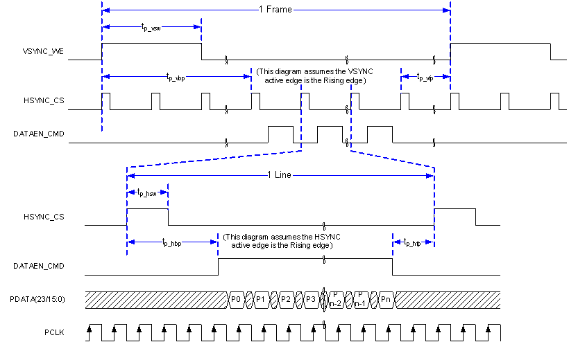 Figure 1. Parallel I/F Frame Timing
 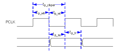 Figure 2. Parallel and BT.656 I/F General Timing
  Figure 3. DLPC2607 PDATA Bus – BT.656 I/F Mode Bit Mapping (YCrCb 4:2:2 Source)
  Figure 4. Flash I/F Timing
 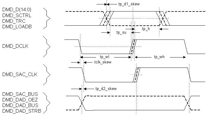 Figure 5. DMD I/F Timing
 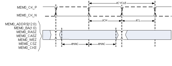 Figure 6. mDRR Memory Address and Control Timing
 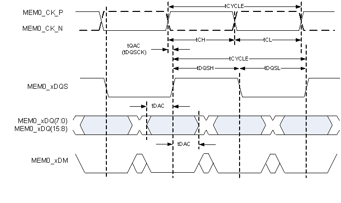 Figure 7. mDRR Memory Write Dtat Timing
 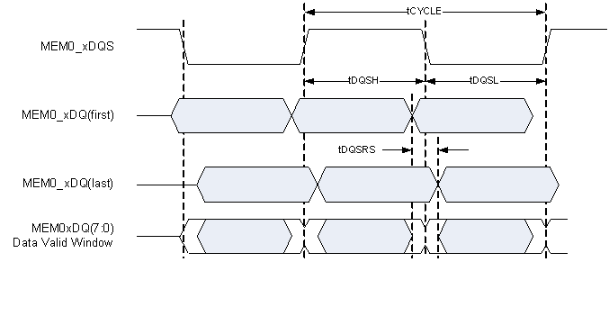 Figure 8. mDDR Memory Read Data Timing