ZHCSC07E December 2013 – March 2019 DLPC2607
PRODUCTION DATA.
- 1 特性
- 2 应用范围
- 3 说明
- 4 修订历史记录
- 5 Pin Configuration and Functions
-
6 Specifications
- 6.1 Absolute Maximum Ratings
- 6.2 ESD Ratings
- 6.3 Recommended Operating Conditions
- 6.4 Thermal Information
- 6.5 Typical Current and Power Dissipation
- 6.6 I/O Characteristics
- 6.7 Internal Pullup and Pulldown Characteristics
- 6.8 Parallel I/F Frame Timing Requirements
- 6.9 Parallel I/F General Timing Requirements
- 6.10 Parallel I/F Maximum Parallel Interface Horizontal Line Rate
- 6.11 BT.656 I/F General Timing Requirements
- 6.12 100- to 120-Hz Operational Limitations
- 6.13 Flash Interface Timing Requirements
- 6.14 DMD Interface Timing Requirements
- 6.15 mDDR Memory Interface Timing Requirements
- 7 Detailed Description
- 8 Application and Implementation
- 9 Power Supply Recommendations
-
10Layout
- 10.1
Layout Guidelines
- 10.1.1 Internal ASIC PLL Power
- 10.1.2 General Handling Guidelines for Unused CMOS-Type Pins
- 10.1.3 SPI Signal Routing
- 10.1.4 mDDR Memory and DMD Interface Considerations
- 10.1.5 PCB Design
- 10.1.6 General PCB Routing (Applies to All Corresponding PCB Signals)
- 10.1.7 Maximum, Pin-to-Pin, PCB Interconnects Etch Lengths
- 10.1.8 I/F Specific PCB Routing
- 10.1.9 Number of Layer Changes
- 10.1.10 Stubs
- 10.1.11 Termination Requirements:
- 10.2 Layout Example
- 10.1
Layout Guidelines
- 11器件和文档支持
- 12机械、封装和可订购信息
请参考 PDF 数据表获取器件具体的封装图。
机械数据 (封装 | 引脚)
- ZVB|176
散热焊盘机械数据 (封装 | 引脚)
7.3.1 Parallel Bus Interface
The parallel bus interface complies with standard graphics interface protocol, which includes a vertical sync signal (VSYNC_WE), horizontal sync signal (HSYNC_CS), optional data valid signal (DATAEN_CMD), a 24-bit data bus (PDATA), and a pixel clock (PCLK). The user can program the polarity of both syncs and the active edge of the clock. Figure 1 shows the relationship of these signals. The data valid signal (DATAEN_CMD) is optional in that the DLPC2607 device provides auto-framing parameters that can be programmed to define the data valid window based on pixel and line counting relative to the horizontal and vertical syncs.
In addition to these standard signals, an optional side-band signal (PDM_CVS_TE) is available, which allows the user to stop the periodic frame updates without losing the displayed image. When PDM_CVS_TE is active, it acts as a data mask and does not allow the source image to be propagated to the display. A programmable PDM polarity parameter determines if it is active high or active low. This parameter defaults to make PDM_CVS_TE active high. Therefore, if this function is not desired, tie it to a logic low on the PCB. PDM_CVS_TE is restricted to change only during vertical blanking. Note that VSYNC_WE must remain active at all times (in Lock-to-VSYNC mode) or the display sequencer stops and causes the LEDs to be shut off.
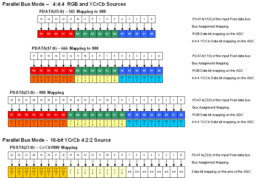
The parallel bus interface supports six data transfer formats:
- 16-bit RGB565
- 18-bit RGB666
- 18-bit 4:4:4 YCrCb666
- 24-bit RGB888
- 24-bit 4:4:4 YCrCb888
- 16-bit 4:2:2 YCrCb (standard sampling assumed to be Y0Cb0, Y1Cr0, Y2Cb2, Y3Cr2, Y4Cb4, Y5Cr4, …)
Figure 9 shows the required PDATA(23:0) bus mapping for these six data transfer formats.
 Figure 9. PDATA Bus – Parallel I/F Mode Bit Mapping