ZHCSCU2E February 2014 – November 2020 DLPC3433 , DLPC3438
PRODUCTION DATA
- 1 特性
- 2 应用
- 3 说明
- 4 Revision History
- 5 Pin Configuration and Functions
-
6 Specifications
- 6.1 Absolute Maximum Ratings
- 6.2 ESD Ratings
- 6.3 Recommended Operating Conditions
- 6.4 Thermal Information
- 6.5 Power Electrical Characteristics
- 6.6 Pin Electrical Characteristics
- 6.7 Internal Pullup and Pulldown Electrical Characteristics
- 6.8 DMD Sub-LVDS Interface Electrical Characteristics
- 6.9 DMD Low-Speed Interface Electrical Characteristics
- 6.10 System Oscillator Timing Requirements
- 6.11 Power Supply and Reset Timing Requirements
- 6.12 Parallel Interface Frame Timing Requirements
- 6.13 Parallel Interface General Timing Requirements
- 6.14 BT656 Interface General Timing Requirements
- 6.15 DSI Host Timing Requirements
- 6.16 Flash Interface Timing Requirements
- 6.17 Other Timing Requirements
- 6.18 DMD Sub-LVDS Interface Switching Characteristics
- 6.19 DMD Parking Switching Characteristics
- 6.20 Chipset Component Usage Specification
-
7 Detailed Description
- 7.1 Overview
- 7.2 Functional Block Diagram
- 7.3 Feature Description
- 7.4 Device Functional Modes
- 7.5 Programming
- 8 Application and Implementation
- 9 Power Supply Recommendations
- 10Layout
- 11Device and Documentation Support
- 12Mechanical, Packaging, and Orderable Information
7.3.1.4 DSI Interface
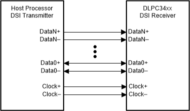
The DLPC34xx controller supports the industry standard DSI (Display Serial Interface) Type-3 LVDS video interface with up to four lanes. DSI is a source-synchronous, high-speed, low-power, low-cost physical layer. The DSI-PHY unit receives data when it operates in high-speed (HS) mode. The DSI-PHY unit receives and transmits data when it operates in low-power (LP) mode for unidirectional data lanes. Point-to-point lane interconnect can be used for either data or clock signal transmission. The high-speed receiver is a differential line receiver circuit. The low-power receiver is an unterminated, single-ended receiver circuit. Figure 7-8 shows a high-level view of the DSI interface.
For a given frame rate, the DSI high-speed (HS) clock frequency must be fixed. If a different DSI clock frequency is ever needed (such as to support another frame rate), an I2C command must be sent to the controller with the updated HS clock frequency.
MIPI refers to the Mobile Industry Processor Interface standard.
Various DSI requirements and features of the DLPC34xx are as follows:
- compliant with the DSI-MIPI Specification for Display Serial Interface (V 1.02.00) except for those items noted in the DSI Host Timing Requirements table
- compliant with D-PHY standard MIPI Specification (V 1.0)
- MIPI DSI Type 3 architecture
- supports display resolutions from 320 × 200 to 1280 × 800
- supports video mode (command mode not supported)
- MIPI DCSSM (Display Command SetSM) commands sent over DSI not supported (send commands via I2C instead)
- supports multiple packets per transmission
- supports trigger messages in the forward direction
- data lanes configurable from one to four channels
- EOT (End of Transfer) command is supported and must be enabled
- CRC (cyclic redundancy check) and ECC
(error correction code) for header supported
- CRC and ECC can be disabled
- checksum for long packets with error reporting (but no ECC)
- supports one virtual channel for video mode
- supports burst mode
- supports non-burst with sync pulses and with sync event
- BTA (bus turn-around) mode not supported and must be disabled in the DSI host processor
- LP mode is required during vertical blanking and vertical sync. LP mode is not supported between pixel lines (i.e. HS blanking must be used for horizontal blanking and horizontal sync)
- an active DSI HS clock is required during LP blanking

The differential DSI clock lane (DCLKN and DCLKP) must be in the LP11 (Idle) state upon the de-assertion of RESETZ (zero-to-one transition) and must remain in this state until HOST_IRQ is de-asserted (one-to-zero transition) to ensure proper DSI initialization.
The controller requires differential data lane '0' (DD0N:DD0P) for DSI operation. The three remaining data lanes are optional depending on the desired input resolution and frame rate. Not all display resolutions and frame rates are supported without using all four data lanes.
The state of GPIO (2:1) pins upon the de-assertion of RESETZ (zero-to-one transition) determines the number of DSI data lanes that are enabled for both LP and HS bus operation.
Only the DLPC3433 controller supports the DSI interface. The DLPC3438 controller does not support the DSI interface.
DSI supported data transfer formats are as follows:
- 24-bit RGB888 - each pixel uses 3 bytes
- 18-bit RGB666 - each pixel packed into 2 or more bytes
- 18-bit RGB666 - each pixel loosely packed into 3 bytes
- 16-bit RGB565 - each pixel uses 2 bytes
- 16-bit 4:2:2 YCbCr - each pixel uses 2 bytes